Guided mode resonance device

a resonance device and guided mode technology, applied in the field of optical devices, can solve the problems of large number of layers, high complexity of the technology to master the optical quality of such devices, and high cost, and achieve the effect of simple, cheap and quick way

Active Publication Date: 2016-12-08
CSEM CENT SUISSE DELECTRONIQUE & DE MICROTECHNIQUE SA RECH & DEV
View PDF12 Cites 17 Cited by
  • Summary
  • Abstract
  • Description
  • Claims
  • Application Information

AI Technical Summary

Benefits of technology

[0055]The method to detect bio-chemical substances according to the invention allows providing a simple, cheap and quick way to detect particular bio-chemical substances. This can be used for example in bio-monitoring or in diagnostics. An example of such bio-chemical substances are antibodies. The method to detect bio-chemical substances according to the invention may use a very basic optical system or may be performed without additional optical components, allowing the detection of one or more bio-chemical substances by simply observing the colors of said outcoupled beams by the eye.
[0056]The invention relates also to a security document and / or a document of value including a said guided mode resonance device as above-mentioned. The color brightness of the outcoupled at least first light beam and second light beam by the guided mode resonance device allows realizing visible security signs, which highly contrasted colors, with optically variable effects such as change of intensity and color with variable angles of illumination and / or observation.

Problems solved by technology

A significant drawback associated with these thin-film optical devices is that very often a large number of layers are needed to obtain a significant optical effect.
The complexity of the technology to master the optical quality of such devices can be considerably high and is thus expensive.
Also, adhesion and stability problems associated with multiple stacked layers may be a problem.
Scattering effects and unwanted reflections inside the optical stack are a current problem especially if special optical effects are to be obtained such as occurring in high quality filters, interferometry or high power laser applications where any stray light may be a limiting factor.
This method cannot be applied in the case of deep grating grooves.
Rosenblatt and Sharon explained in these papers that the efficient transfer of wave energy between forward and backward propagations at resonance is due to the relative phase-shift between the incident and the diffracted waves, resulting in destructive and constructive interference of forward and backward propagating waves.
Limitations of resonating waveguide structures are particularly linked with the fact that specular reflection phenomena reduce the performances of filters.
These specular reflection effects may also limit the performance of resonating waveguide structures when they are used to produce specific colors.
A limitation of guided mode resonance devices in sensors is that the interaction length of the waves interacting with said substances is limited and thus the effects obtained are small.
In such a device the major drawback is the inherent leakage of light along the waveguide, therefor the resonant light cannot be absorbed completely.

Method used


Image

  • Guided mode resonance device
  • Guided mode resonance device
  • Guided mode resonance device

Examples


Embodiment Construction

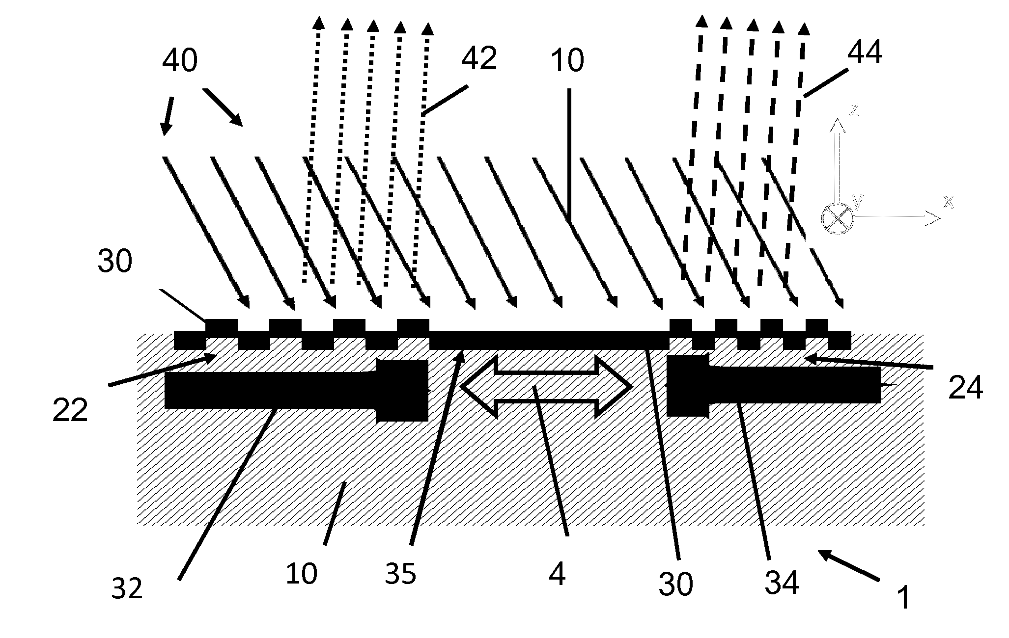
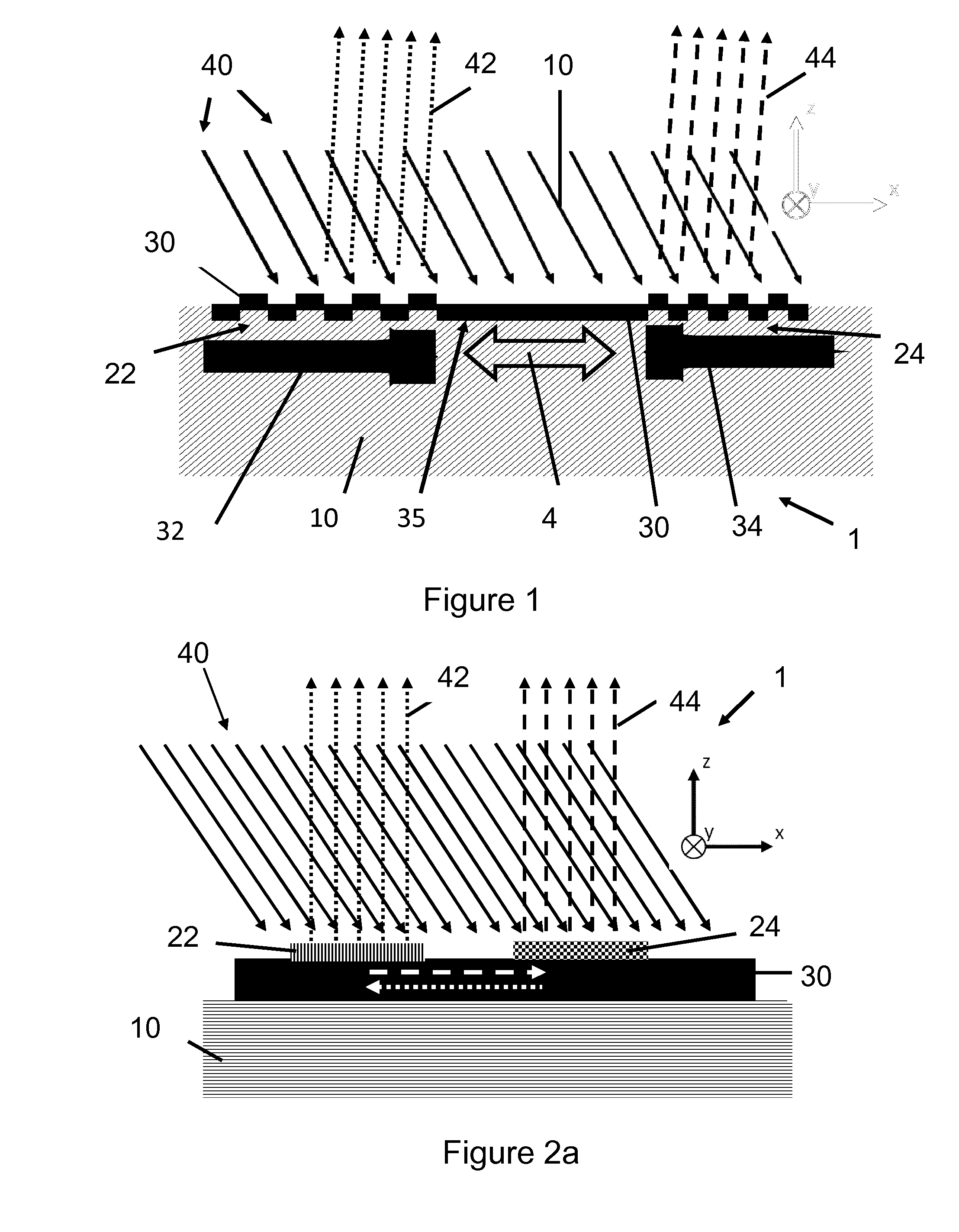
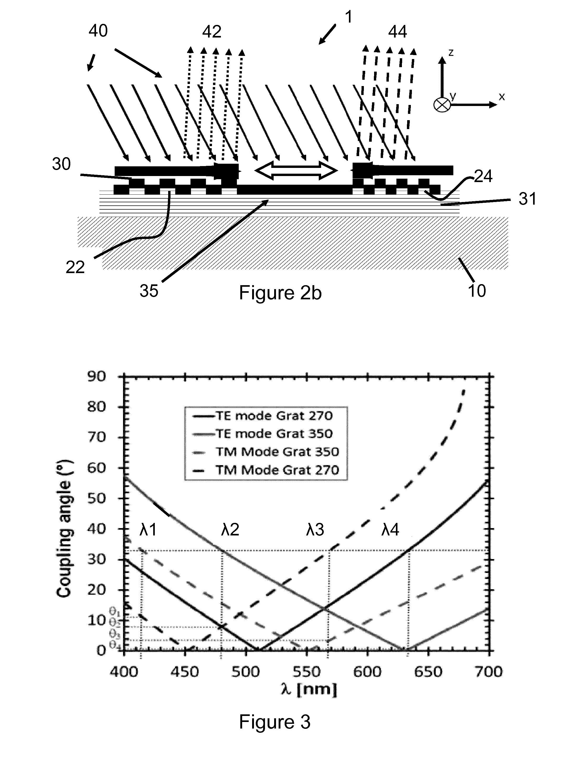
[0072]Resonating waveguide gratings (RWG), also called leaky mode filters or also guided-mode resonance filters or guided-mode resonance devices are well described in the literature. The functional principle of these devices is based on a resonance phenomenon that may occur in waveguide grating structures. Resonant waveguide gratings consist of a combination of a subwavelength grating and a thin film waveguide. The subwavelength grating acts as an incoupling grating for the waveguide. A resonance occurs when a portion of the incident light, diffracted by the grating, matches a mode of the waveguide. As most of the spectrum of the incident light on the grating does not couple into the waveguide, strong spectral changes may be observed in reflection and / or transmission. The resonance effects, their theoretical explanation and their applications have been extensively described in the past and will not be further commented here. Relevant information on this subject may be found in the f...


PUM

PropertyMeasurementUnit
refractive indexaaaaaaaaaa
incident angleaaaaaaaaaa
thicknessaaaaaaaaaa

Abstract

A guided mode resonance device, comprising—a substrate,—a waveguide,—a grating structure associated with said waveguide, said grating structure being arranged to an incident surface of said substrate, said incident surface being intended to receive an incident light beam provided by at least one light source, said incident light beam having an incident angle, defined relative to the normal of said waveguide, said grating structure comprising at least one elementary structure comprising at least a first-type grating structure and at least a second-type grating structure,—wherein:—said waveguide is arranged to transfer light from_the first-type grating structures to the second-type grating structure and also to transfer light from the second-type grating structures to the first-type grating structure,—said first-type grating structure is arranged to couple out a first light beam,—said second-type grating structure is arranged to couple out a second light beam,—said first light beam having a different spectral distribution than said second light beam.

Description

TECHNICAL FIELD[0001]The invention relates to the field of optical devices, more particularly to devices that incorporate optical waveguides. It more specifically relates to guided mode resonance devices and their application in optical sensors, optical filters and security devices.BACKGROUND OF HE INVENTION[0002]The field of thin-film optics is an important area in optical technologies. A huge variety of filters and optical devices are produced and used in numerous industries and for a wide range of applications. Most of these thin-film optical structures, assemblies and devices consist of homogeneous layers deposited with precisely controlled thicknesses and material parameters and they are most often realized in a low pressure atmosphere needing a sophisticated technology. Examples of devices using such multilayer filters include, but are not limited to, antireflection filters, low-and high pass filters, phase plates, flat beamsplitters, polarization filters, micromirrors. In sev...

Claims


Application Information

Patent Timeline
Patent Type & Authority Applications(United States)
IPC IPC(8): G02B6/124G01N21/77G02B6/34G02B6/293G02B5/18G02B27/42
CPCG02B6/124G02B5/1809G01N21/7743G02B6/34G02B6/29325G02B27/4272G02B5/203G02B6/12007G02B2006/12107
Inventor DAVOINE, LAURENTBASSET, GUILLAUME
Owner CSEM CENT SUISSE DELECTRONIQUE & DE MICROTECHNIQUE SA RECH & DEV
Why Eureka
Try Eureka