

Method for manufacturing amoled display device and structure thereof
- Summary
- Abstract
- Description
- Claims
- Application Information
AI Technical Summary
Benefits of technology
Problems solved by technology
Method used
Image

Examples
Embodiment Construction
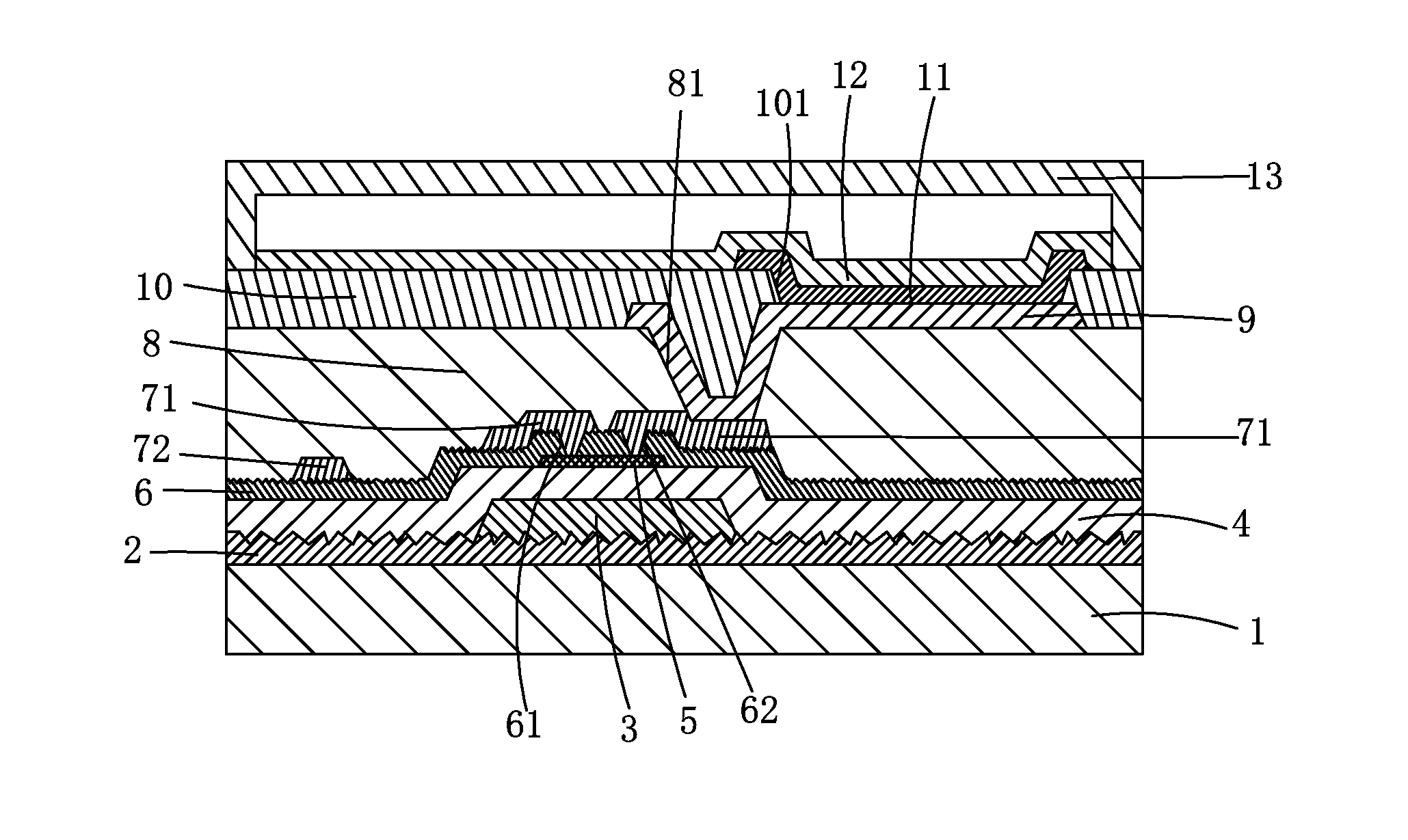
[0074]To further expound the technical solution adopted in the present invention and the advantages thereof, a detailed description is given to a preferred embodiment of the present invention and the attached drawings.
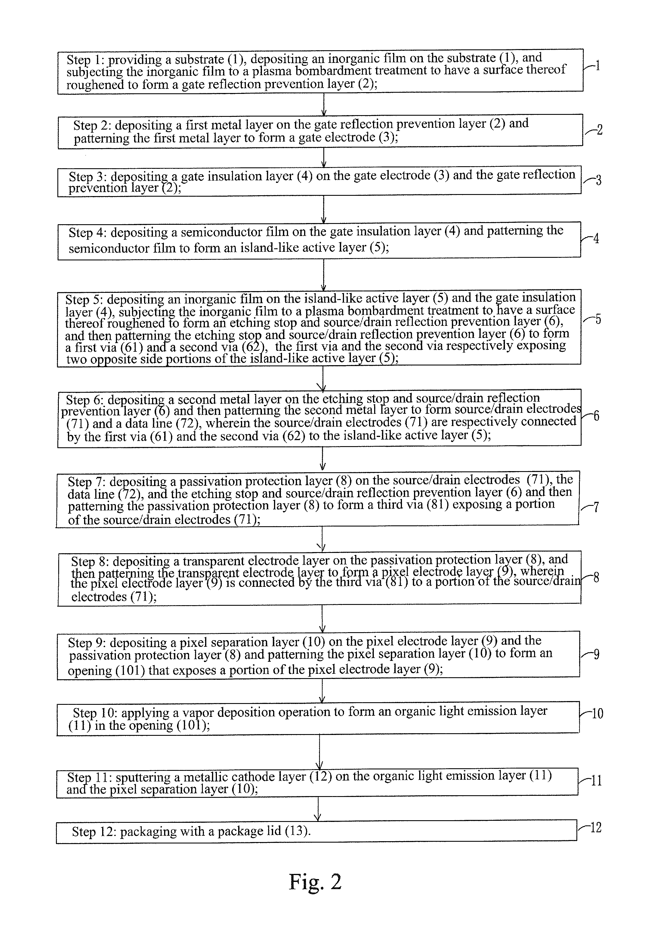
[0075]Referring to FIG. 2, firstly, the present invention provides a method for manufacturing an active matrix organic light emitting diode (AMOLED) display device, comprising the following steps:
[0076]Step 1: as shown in FIG. 3, providing a substrate 1, depositing an inorganic film having a thinly distributed thin material on the substrate 1, and subjecting the inorganic film to a plasma bombardment treatment to have a surface thereof roughened to form a gate reflection prevention layer 2.
[0077]Specifically, the substrate 1 of Step 1 is preferably a glass substrate; the inorganic film is formed of a material of silicon dioxide (SiO2) and has a thickness of 1000-3000 Å; and the plasma bombardment treatment uses a gas of nitrogen (N2), oxygen (O2), or nitrogen dioxide (...
PUM
 Abstract
Description
Claims
Application Information