Antenna Unit and Terminal
- Summary
- Abstract
- Description
- Claims
- Application Information
AI Technical Summary
Benefits of technology
Problems solved by technology
Method used
Image

Examples
embodiment 1
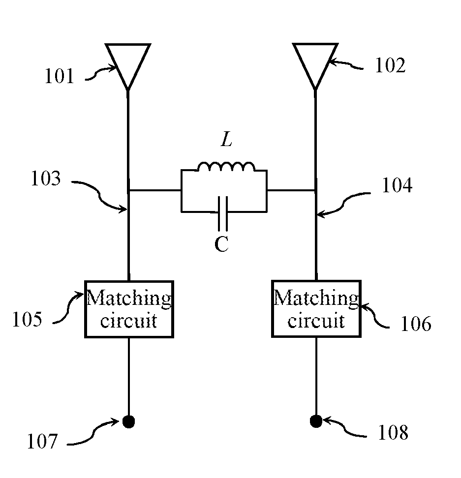
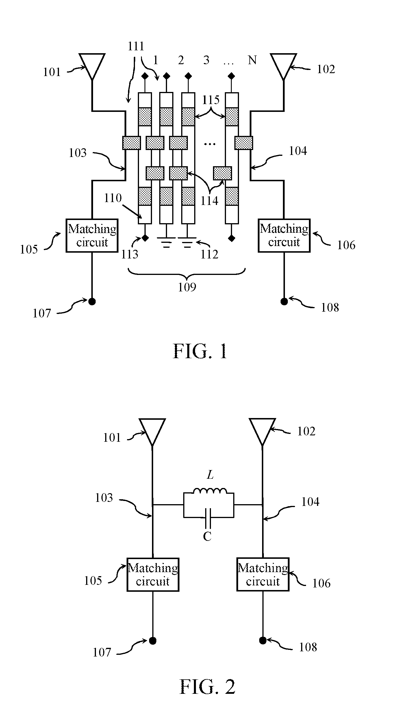
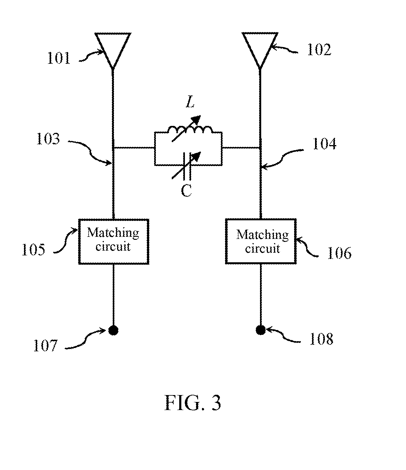
[0027]This embodiment provides an antenna unit, comprising: an antenna circuit board, at least two neighboring antennas and an electromagnetic coupling module used to isolate coupling signal transmission between two neighboring antennas, wherein the electromagnetic coupling module is connected in series between the two neighboring antennas. In this embodiment, the electromagnetic coupling module comprises an isolation metal structure and lumped parameter elements; and the isolation metal structure is respectively connected with the two neighboring antennas in series through the lumped parameter elements, the isolation metal structure includes at least one independent metal subpart, the metal subparts are connected through the lumped parameter element(s), one end of the metal subpart is floating or is open-circuited, and the other end of the metal subpart is grounded or short-circuited.
[0028]The antenna unit provided by this embodiment adopts the following isolation technology: the i...
embodiment 2
[0040]In this embodiment, the antenna unit is applied to LTE low frequency band 4 MIMO high-isolation antenna design of the terminal. Specifically, as illustrated in FIG. 4, the four antennas in this embodiment are Inverted F Antennas (IFAs) printed on two surfaces of a Planar Circuit Board (PCB). The size of the entire PCB is 80×210 mm, and the thickness is 1 mm. FIG. 4(a) illustrates a PCB surface layer trace form and FIG. 4(b) illustrates a PCB bottom layer trace form. As illustrated, traces of an antenna 1 (301 as illustrated) and an antenna 2 (302 as illustrated) are located at an upper part of a surface of a surface layer of the PCB and are distributed in mirror symmetry with respect to a long axis of the PCB. An antenna 3 (303 as illustrated) and an antenna 4 (304 as illustrated) are located at a lower part of a surface of a bottom layer of the PCB and are distributed in mirror symmetry with respect to the long axis of the PCB. Feed points 305, 305, 307, 308 are respectively ...
embodiment 3
[0046]As illustrated in FIG. 11, this embodiment provides a terminal, comprising the antenna unit provided by embodiment 1 or embodiment 2, a main circuit board and an operating circuit of the terminal, wherein the operating circuit of the terminal is arranged on the main circuit board of the terminal and the antenna unit is connected with the main circuit board.
[0047]In order to reduce signal interference between antennas on the antenna circuit board and the operating circuit on the main circuit board, at the terminal provided by this embodiment, a spacer may be arranged between the main circuit board and the antenna mainboard.
[0048]As illustrated in FIG. 12 which is a schematic diagram of a four-antenna terminal provided by this embodiment, due to the difficulty in the design of LTE low-frequency 700 MHz 4 MIMO antennas, in order to guarantee the high isolation between any two antennas, the high isolation technology of the present invention is adopted and slitting treatment needs ...
PUM
 Abstract
Description
Claims
Application Information
 - Generate Ideas
- Intellectual Property
- Life Sciences
- Materials
- Tech Scout
- Unparalleled Data Quality
- Higher Quality Content
- 60% Fewer Hallucinations
Browse by: Latest US Patents, China's latest patents, Technical Efficacy Thesaurus, Application Domain, Technology Topic, Popular Technical Reports.
© 2025 PatSnap. All rights reserved.Legal|Privacy policy|Modern Slavery Act Transparency Statement|Sitemap|About US| Contact US: help@patsnap.com