Composite quantum-dot materials for photonic detectors

a quantum-dot detector and composite technology, applied in the field of photodetectors, can solve the problems of spectrally limited imaging platforms and very high cost, and achieve the effects of stabilizing the local density of states, reducing the rate of local reaction to atmospheric oxygen, and stabilizing the electrical properties of devices

Active Publication Date: 2017-01-19
LADARSYST INC
View PDF17 Cites 18 Cited by
  • Summary
  • Abstract
  • Description
  • Claims
  • Application Information

AI Technical Summary

Benefits of technology

[0005]The present disclosure is directed to apparatus and methods of manufacturing composite pixelated quantum-dot photodetector arrays. One apparatus of the present disclosure includes a composite quantum-dot photodetector comprising a substrate with a colloidally deposited thin film structure forming a photosensitive region, the thin film containing at least one type of a nanocrystal quantum-dot, whereby the nanocrystal quantum dots are spaced by ligands to form a lattice, and the lattice of the quantum dots has an infill material that forms an inorganic matrix that isolates the nanocrystal quantum dots from atmospheric exposure. In one aspect, a method of manufacturing the aforementioned photodetector comprises the following steps; alternatively dipping a wafer, or other substrate, into a colloidal solution containing at least one type of a quantum dot, thereby forming a monolayer of the quantum dots and then dipping the substrate with the monolayer of the quantum dots into a ligand spacing solution to build a film of the quantum dots; and alternatively exposing the film of the quantum dots to a gas vapor and a metalorganic precursors material. Exposing the film to the vapor coats the film's accessible surfaces, reacting with the infill material. Exposing the film to the inorganic matrix material penetrates pores of the film and reacts with the film's accessible surfaces to form an inorganic matrix. The inorganic matrix isolates the quantum dots from atmospheric exposure, reducing the rate of local reaction to atmospheric oxygen, thereby stabilizing the electrical properties of the device and stabilize the local density of states on the quantum dot surface. Also, the infill semiconductor can provide a bandgap heterostructure interface to the quantum-dot, preserving local confinement of one or both of the charge carriers, or promoting preferable injection or extraction of holes or electrons, into or out of the infill, or promoting preferential tunneling or hopping transport between quantum-dots.

Problems solved by technology

Due to silicon's band gap, these imaging platforms are spectrally limited with primary applications in the human visible spectrum.
These compound semiconductor materials demonstrate good image performance, but they do so at very high cost due to manufacturability and cost structure due to their incompatibility with commercial high volume CMOS silicon processes.

Method used


Image

  • Composite quantum-dot materials for photonic detectors
  • Composite quantum-dot materials for photonic detectors
  • Composite quantum-dot materials for photonic detectors

Examples


Embodiment Construction

[0018]Referring now to the drawings, wherein like components are designated by like reference numerals. Methods of manufacture and various embodiments of the present disclosure are described further herein below.

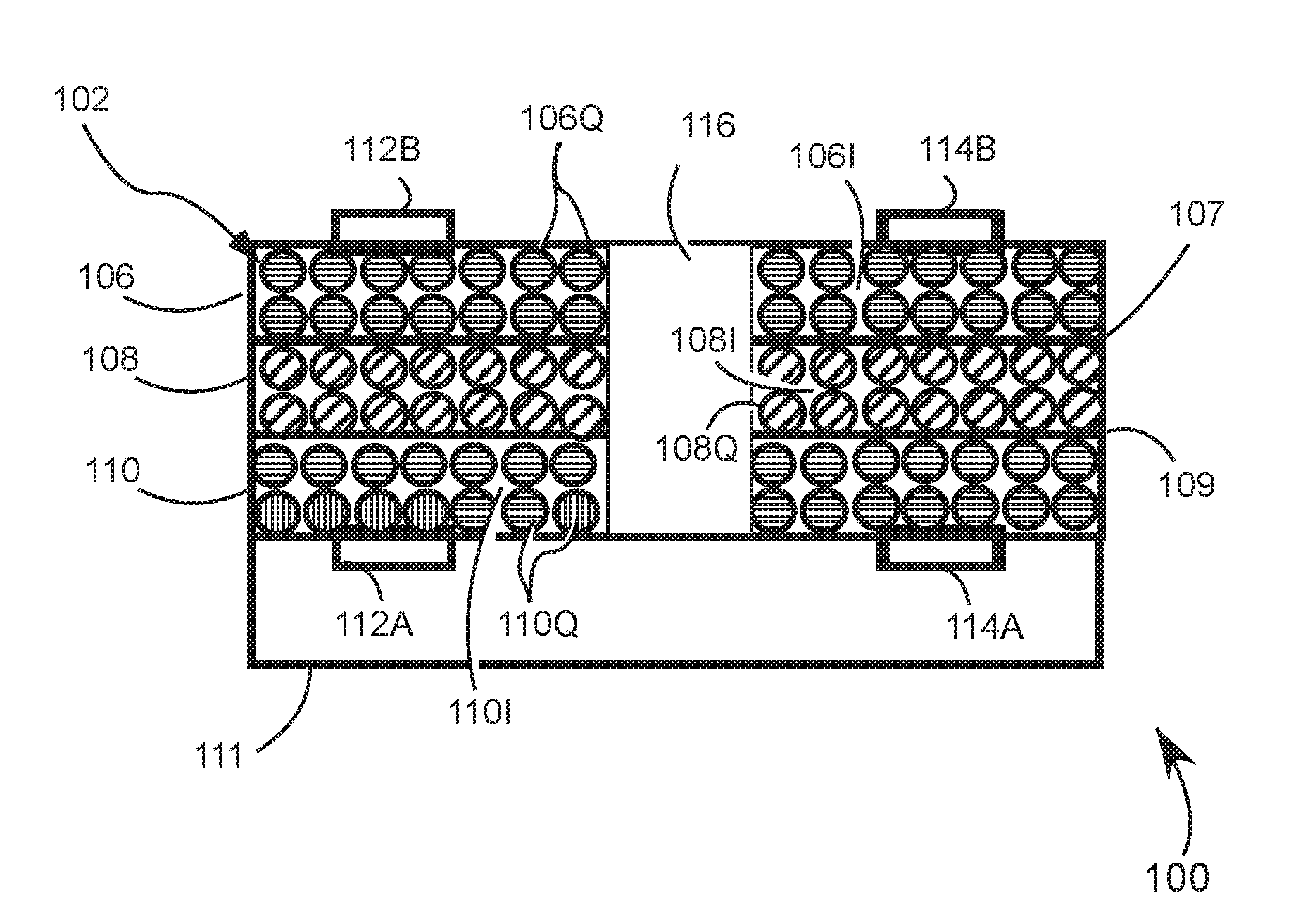
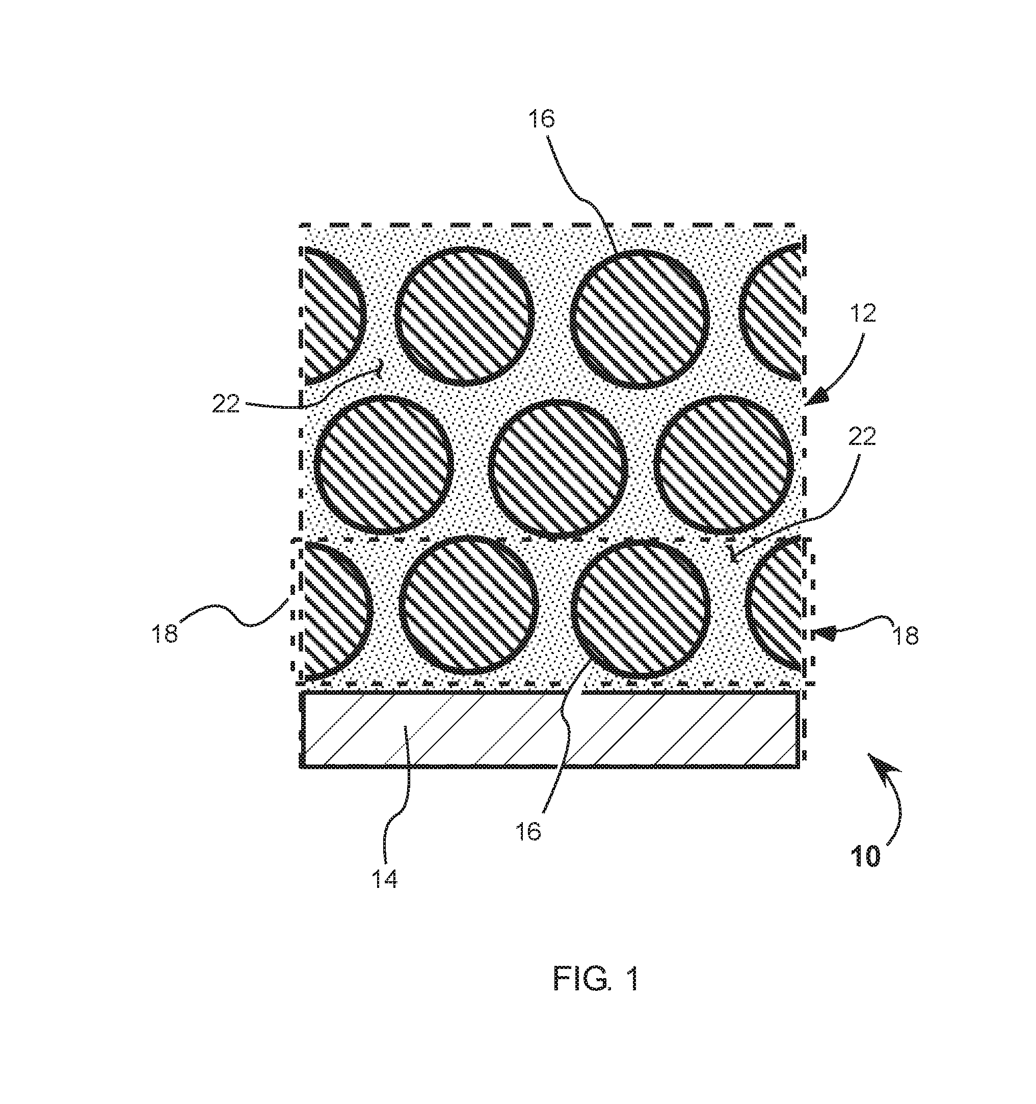
[0019]Referring to FIG. 1, a partial view of a cross-section of a composite quantum-dot photodetector film 10 has a photodetector film 12 formed by a layer-by-layer deposition process to build homogenous and heterogeneous photodetector film on a substrate 14. One such process includes alternatively dipping the substrate 14 into a colloidal solution containing at least one type of a quantum dot 16, thereby forming a monolayer 18 of quantum dots 16 and then dipping the substrate with monolayer 18 of quantum dots 16 in a ligand spacing solution to build a lattice of the quantum dots. Then, alternatively exposing the lattice of the quantum dots to a water vapor and an infill materials leaves behind an inorganic material 22, wherein exposing the film to the water vapor coats the ...


PUM

PropertyMeasurementUnit
peak-to-peak flatnessaaaaaaaaaa
wavelengthsaaaaaaaaaa
carrier mobilitiesaaaaaaaaaa

Abstract

A composite quantum-dot photodetector comprising a substrate with a colloidally deposited thin film structure forming a photosensitive region, the thin film containing at least one type of a nanocrystal quantum-dot, whereby the nanocrystal quantum dots are spaced by ligands to form a lattice, and the lattice of the quantum dots has an infill material that forms an inorganic matrix that isolates the nanocrystal quantum dots from atmospheric exposure.

Description

CROSS-REFERENCE TO RELATED APPLICATIONS[0001]This application is a continuation-in-part of U.S. patent application Ser. No. 14 / 967,247 filed on Dec. 11, 2014 which claims benefit of U.S. provisional patent application No. 62 / 090,776 filed on Dec. 11, 2014.GOVERNMENT INTEREST STATEMENT[0002]This invention was made with government support under Contract H92222-12-P-0068 awarded by the United States Special Operations Command. The government has certain rights in the invention.TECHNICAL FIELD OF THE DISCLOSURE[0003]The present disclosure relates in general to photodetectors. This application relates in particular to methods of manufacturing composite quantum-dot photodetectors.BACKGROUND DISCUSSION[0004]CMOS silicon imagers are the dominant focal plane arrays for visible light imaging. CMOS silicon imagers are implemented in multitude of applications from security cameras to cell phones. Due to silicon's band gap, these imaging platforms are spectrally limited with primary applications...

Claims


Application Information

Patent Timeline
Patent Type & Authority Applications(United States)
IPC IPC(8): H01L31/0352H01L31/18H01L31/0224H01L31/02H01L27/144
CPCH01L31/035263H01L31/035218H01L31/02019H01L27/1446H01L31/022466B82Y20/00Y10S977/774Y10S977/813Y10S977/892Y10S977/954B82Y40/00H01L31/18H01L27/14601H01L31/1876H01L31/0264H01L31/101H01L31/109Y02E10/549H10K30/00
Inventor WILLIAMS, GEORGEHUNTINGTON, ANDREW S.
Owner LADARSYST INC
Why Eureka
Try Eureka