Substrate for light emitting devices and light emitting device

a technology of light emitting devices and substrates, which is applied in the direction of semiconductor devices for light sources, lighting and heating apparatus, planar light sources, etc., can solve the problems of increased size of substrates, difficult to realize commercially, and strength of ceramic substrates, and achieve excellent mass productivity and high light reflectivity.

Active Publication Date: 2017-01-19
SHARP KK
View PDF3 Cites 12 Cited by
  • Summary
  • Abstract
  • Description
  • Claims
  • Application Information

AI Technical Summary

Benefits of technology

[0043]According to the aspect of the invention, it is possible to provide a substrate for light emitting devices having heat radiating properties, dielectric strength voltage properties, high light reflectivity, and excellent mass productivity.

Problems solved by technology

However, increasing a size of a ceramic substrate has been attempted in order to realize a larger size on a commercial basis in accordance with the requirements of an increase in size of a ceramic substrate, but a larger size thereof is difficult to realize on a commercial basis due to three problems of strength, manufacturing precision, and manufacturing cost of a ceramic substrate.
Specifically, since a ceramic material is normally a piece of pottery, a problem regarding strength of a ceramic substrate occurs, when a size thereof is increased.
When a thickness of a substrate is increased in order to solve this problem, new problems occur such that heat resistance increases (heat radiating properties are deteriorated) and a material cost of a ceramic substrate also increases.
When a size of a ceramic substrate is increased, not only external dimensions of a ceramic substrate, but dimensions of an electrode pattern formed on a ceramic substrate are also likely changed, and this may easily result in a decrease in manufacturing yield of a ceramic substrate and an increase in manufacturing cost of a ceramic substrate.
An increase in the number of light emitting elements to be mounted on a ceramic substrate is also a problem along with the problems associated with an increase in size of a ceramic substrate.
For example, in the light emitting device described above, the number of light emitting elements mounted on one ceramic substrate is extremely large, as much as 400 or more, and this is a reason for a decrease in manufacturing yield.
However, in a case of using an organic resist as an insulating layer in a substrate for light emitting devices in the related art, sufficient thermal conductivity, heat resistance, and light resistance are not obtained and dielectric strength voltage properties necessary for a substrate for high-output light emitting devices are not obtained.

Method used


Image

  • Substrate for light emitting devices and light emitting device
  • Substrate for light emitting devices and light emitting device
  • Substrate for light emitting devices and light emitting device

Examples


embodiment 1

Configuration of Lighting Device 1

[0067]Embodiment 1 will be described as follows with reference to FIG. 1 to FIG. 8.

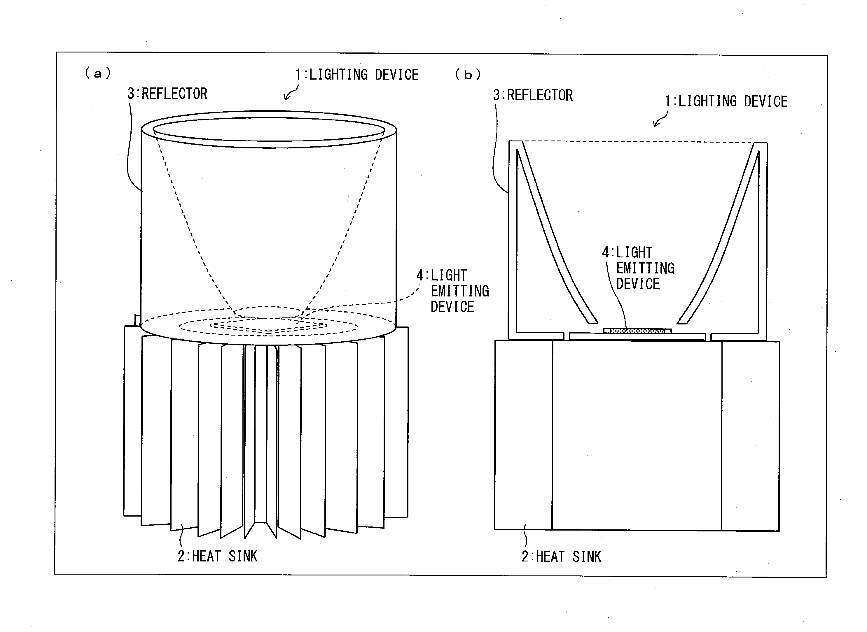
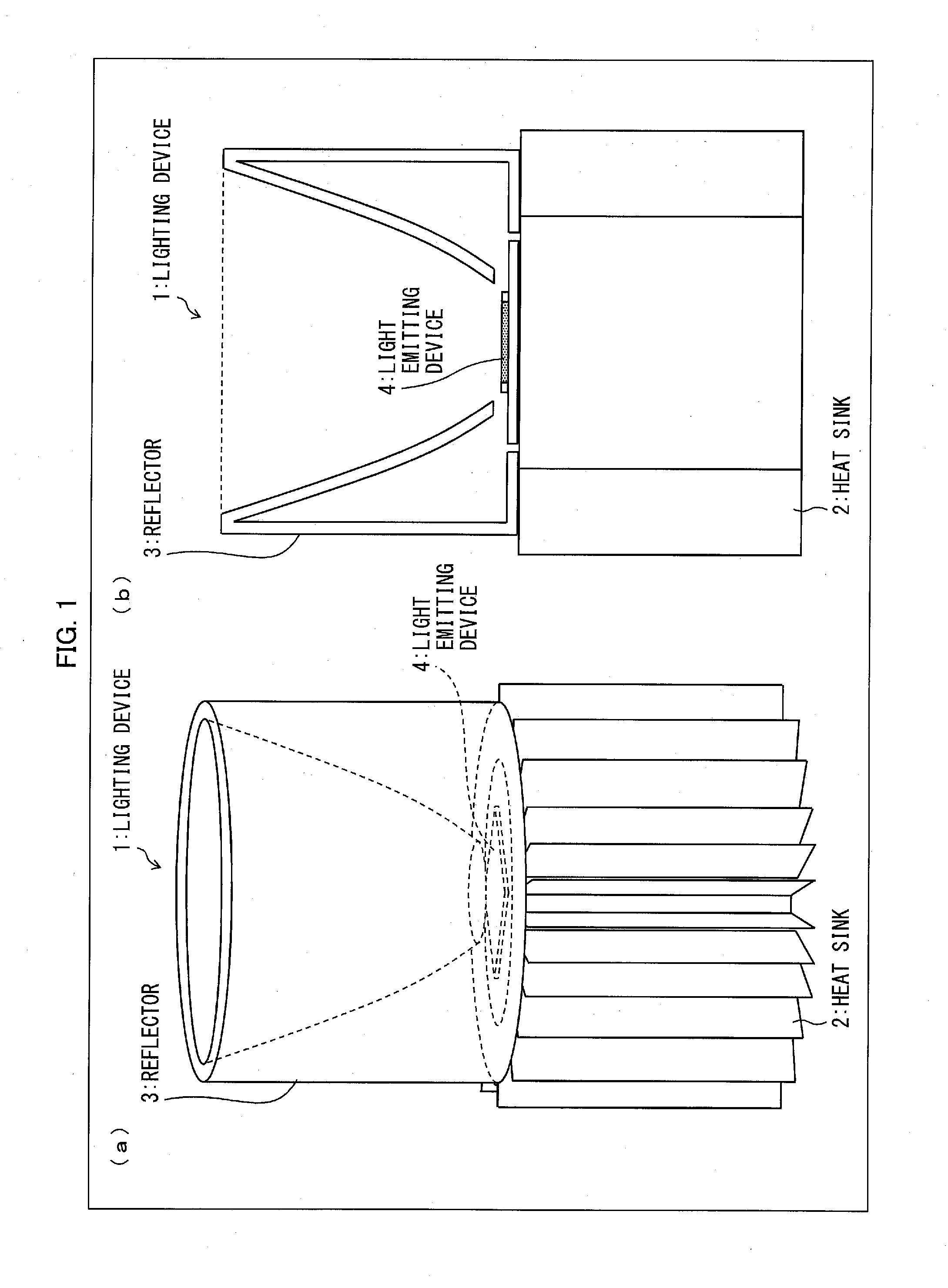
[0068]FIG. 1(a) is a perspective view showing appearance of a lighting device 1 according to Embodiment 1 and FIG. 1(b) is a sectional view of the lighting device 1. The lighting device 1 includes a light emitting device 4, a heat sink 2 for radiating heat generated from the light emitting device 4, and a reflector 3 which reflects light emitted from the light emitting device 4. FIG. 1 shows an example in which the light emitting device 4 according to Embodiment 1 is applied to the lighting device 1.

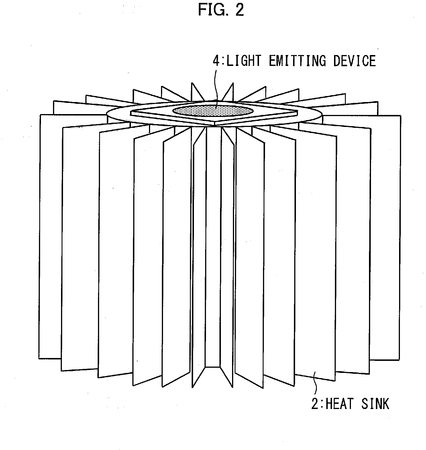
[0069]FIG. 2 is a perspective view of appearance of the light emitting device 4 and the heat sink 2 according to Embodiment 1. The light emitting device 4 may be used to be mounted on the heat sink 2.

[0070](Configuration of Light Emitting Device 4)

[0071]FIG. 3(a) is a plan view showing a configuration of the light emitting device 4 and FIG. 3(b) is a sectional view taken a...

modified example of embodiment 1

[0171]A modified example of Embodiment 1 of the invention will be described as follows with reference to FIG. 19. FIG. 19 is a diagram for illustrating a configuration of the substrate 5 according to a modified example of the substrate 5 of Embodiment 1. FIG. 19(a) is a plan view of the substrate 5 according to the modification example of Embodiment 1, FIG. 19(b) is a sectional view taken along an arrow B-B shown in FIG. 19(a), and FIG. 19(c) is an enlarged view of a part of FIG. 19(b).

[0172]As shown in FIG. 19(c), the substrate 5 according to the modification example of Embodiment 1 is different from the substrate 5 according to Embodiment 1 in that a buffer layer 250 is formed between the base 10 (base) and the intermediate layer 11. The other configurations of the substrate 5 according to the modification example of Embodiment 1 are the same as those of the substrate 5 according to Embodiment 1.

[0173]According to the substrate 5 according to Embodiment 1, the intermediate layer 1...

embodiment 2

[0187]Embodiment 2 of the invention will be described as follows with reference to FIG. 9 to FIG. 11. For convenience of description, the same reference numerals are used for the members having the same functions as the members described in the embodiment described above and the description thereof will be omitted.

[0188]FIG. 9(a) is a plan view showing a configuration of a substrate 5A according to Embodiment 2, FIG. 9(b) is a sectional view taken along a surface CC shown in FIG. 9(a), and FIG. 9(c) is an enlarged view of a part of the sectional view. In the same manner as the substrate 5 according to Embodiment 1, the substrate 5A according to embodiment 2 is applied to the light emitting device 4 of FIG. 3 and can be applied to the lighting device 1 of FIG. 1.

[0189]In Embodiment 1 described above, the intermediate layer 11, the reflective layer 12, and the protective layer 13 are formed on the aluminum base 10. The intermediate layer 11 is formed between the aluminum base 10 and t...


PUM

PropertyMeasurementUnit
thicknessaaaaaaaaaa
sizeaaaaaaaaaa
sizeaaaaaaaaaa

Abstract

In order to provide a substrate for light emitting devices having high heat radiating properties, dielectric strength voltage properties, light reflectivity, and excellent mass productivity, a substrate (5) includes an intermediate layer (11) containing ceramic which is formed on the surface of the aluminum base (10) by using an aerosol deposition method.

Description

TECHNICAL FIELD[0001]The present invention relates to a substrate for light emitting devices, a light emitting device using the substrate for light emitting devices, and a manufacturing method of a substrate for light emitting devices. The invention particularly relates to a substrate for light emitting devices having high dielectric strength voltage properties and heat radiating properties.BACKGROUND ART[0002]High reflectivity, high heat radiating properties, dielectric strength voltage, and long-term reliability can be exemplified as basic properties necessary for a substrate for light emitting devices. High dielectric strength voltage properties are particularly necessary for a substrate for light emitting devices used in high-intensity lighting.[0003]In the related art, a light emitting device including a ceramic substrate or a substrate including an organic resist layer on a metal base as an insulating layer has been known as a substrate for light emitting devices. Hereinafter,...

Claims


Application Information

Patent Timeline
Patent Type & Authority Applications(United States)
IPC IPC(8): H01L33/64H01L33/56H01L33/62H01L33/60H01L25/075
CPCH01L33/642H01L33/60H01L33/641H01L25/0753H01L2933/005H01L33/56H01L2933/0075H01L2933/0058H01L2933/0066H01L33/62F21K9/00F21V29/773H01L2224/16225H05K1/053H05K3/44H05K2201/0179H05K2201/10106F21Y2105/10F21Y2115/10
Inventor KONISHI, MASAHIROITOH, SHINNOKUBO, HIROYUKIITAKURA, YOSHIAKI
Owner SHARP KK
Why Eureka
Try Eureka