Substrate processing apparatus, substrate processing system. and substrate processing method

a substrate processing and substrate technology, applied in the direction of manufacturing tools, semiconductor/solid-state device testing/measurement, lapping machines, etc., can solve the problems of becoming increasingly strict requirements, and achieve the effect of improving the controllability of the etching of the substra

Active Publication Date: 2017-02-16
EBARA CORP
View PDF6 Cites 40 Cited by
  • Summary
  • Abstract
  • Description
  • Claims
  • Application Information

AI Technical Summary

Benefits of technology

[0011]A first aspect of the present invention provides a substrate processing apparatus for processing a processing target region (a semiconductor material) on a substrate by bringing the substrate and a catalyst into contact with each other in the presence of processing liquid. This substrate processing apparatus includes a substrate holding unit configured to hold the substrate, a catalyst holding unit configured to hold the catalyst, and a driving unit configured to move the substrate holding unit and the catalyst holding unit relative to each other with the processing target region on the substrate and the catalyst kept in contact with each other. The catalyst holding unit includes an elastic member for holding the catalyst. According to this aspect, when the processing target region on the substrate and the catalyst are brought into contact with each other, the elastic member is deformed, which allows the catalyst to evenly contact the substrate in conformity with the shape of the substrate (warpage and the like of the substrate), thereby allowing a uniform etching rate within the contat area.
[0089]According to a seventy-ninth aspect of the present invention, in any one of the seventy-third to seventy-eighth aspects, the catalyst is electrically divided into a plurality of regions, and is configured to allow a different voltage to be applied for each of the plurality of regions. According to this aspect, the active status of the surface of the catalyst can be changed by the application of the voltage varying for each region of the catalyst, which leads to an ability to change the etching rate of substrate for each region, thereby improving controllability of the etching of the substrate.

Problems solved by technology

In recent years, the planarization technique including the CMP has been facing expansion of a variety of possible polishing target materials, and also has been subject to requirements that has been becoming increasingly stricter with respect to a polishing capability thereof (for example, flatness, a damage incurred from the polishing, and further, productivity).

Method used


Image

  • Substrate processing apparatus, substrate processing system. and substrate processing method
  • Substrate processing apparatus, substrate processing system. and substrate processing method
  • Substrate processing apparatus, substrate processing system. and substrate processing method

Examples


first embodiment

A. First Embodiment

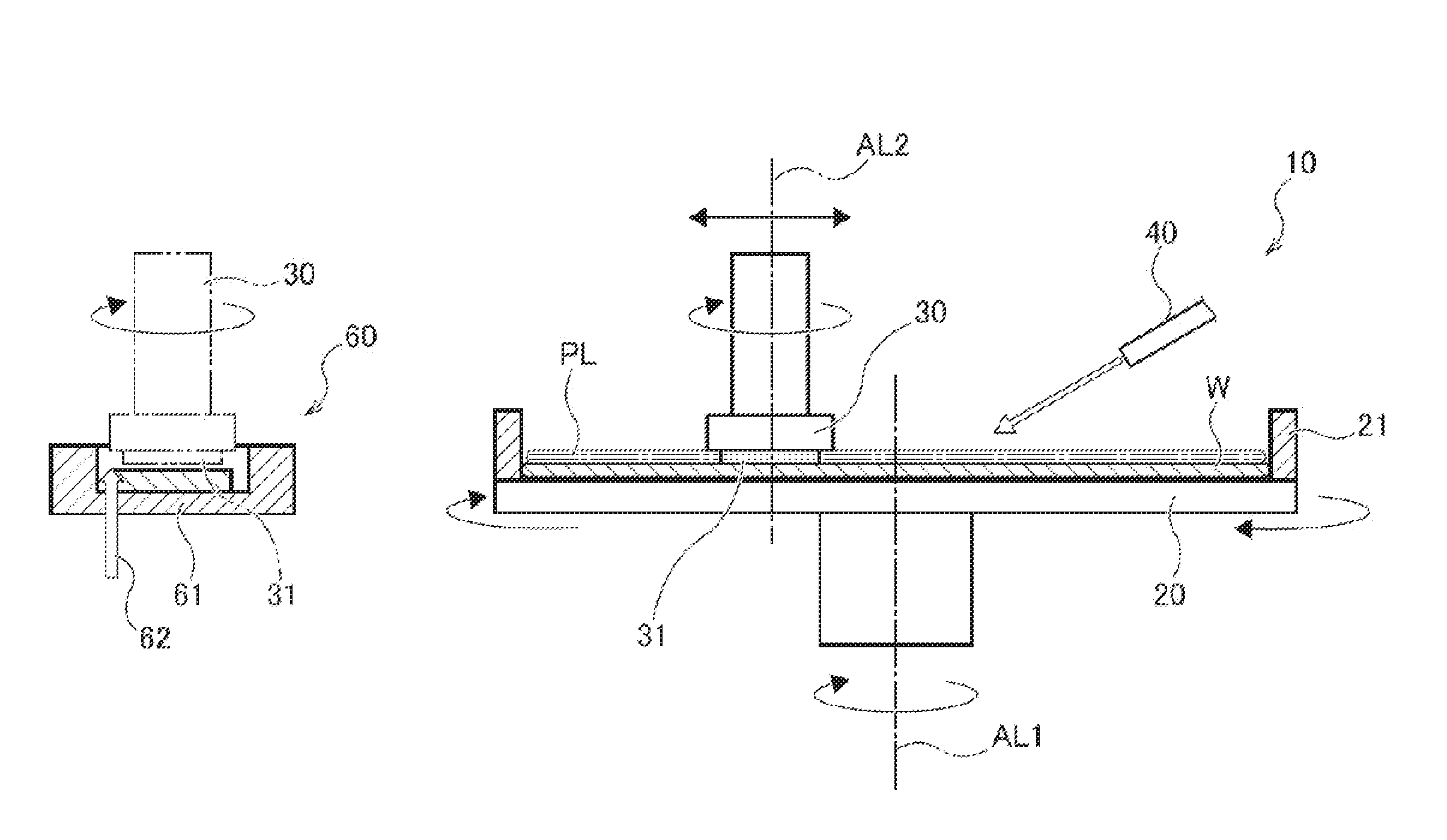
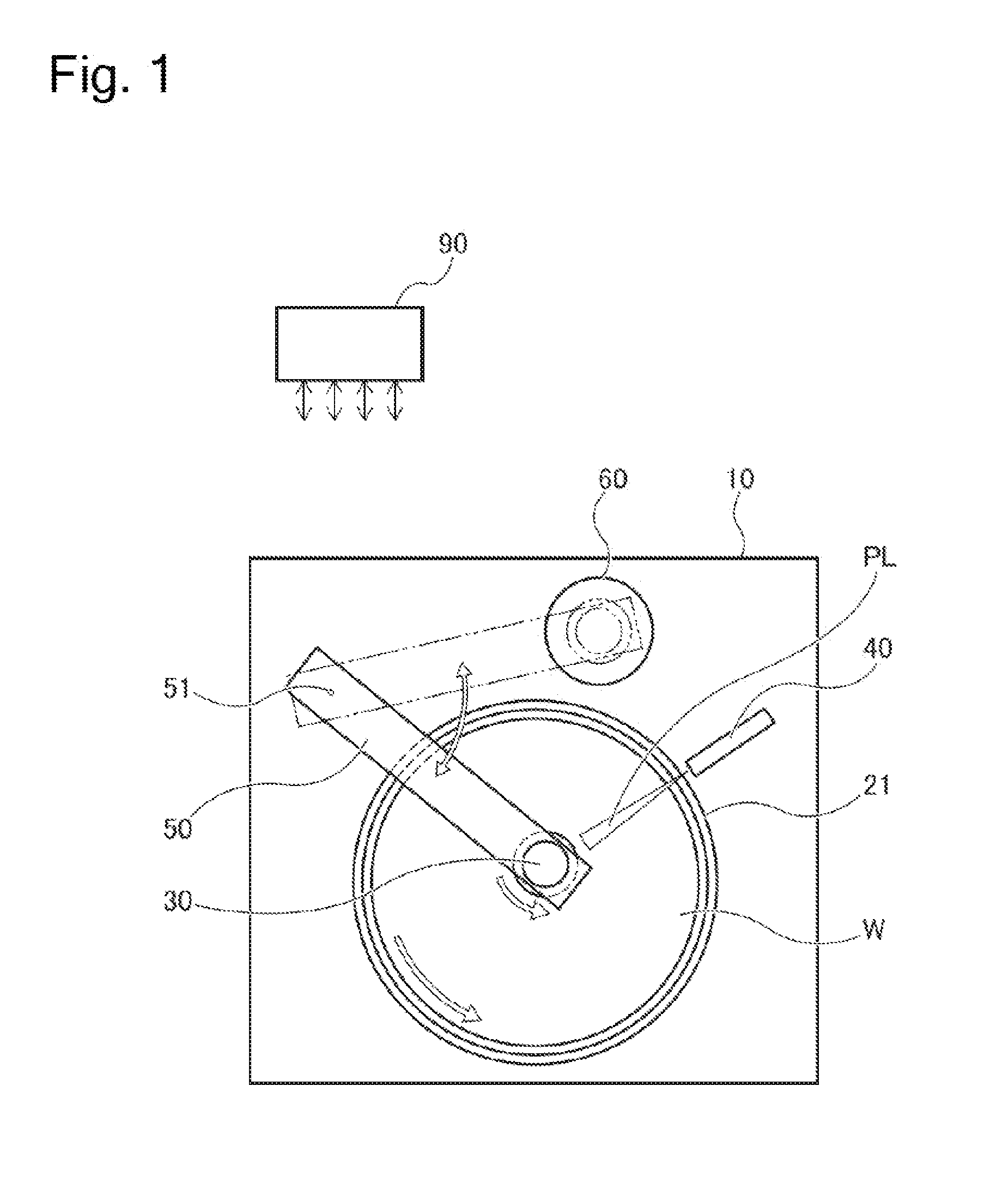
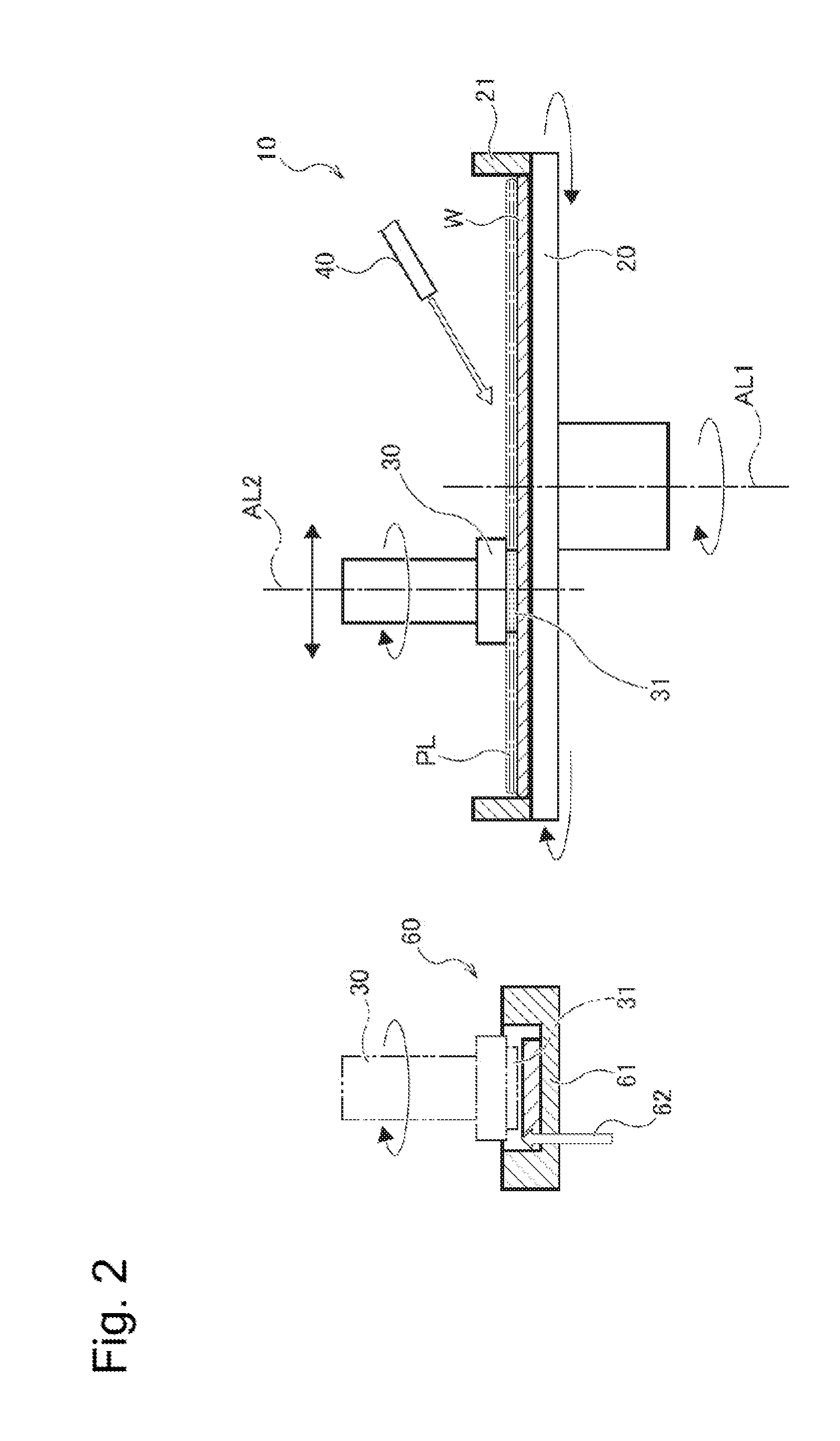
[0219]FIG. 1 is a schematic plan view of a substrate processing apparatus 10 of a substrate processing system as one embodiment of the present invention. FIG. 2 is a side view of the substrate processing apparatus 10 illustrated in FIG. 1. The substrate processing apparatus 10 is an apparatus that performs etching processing on a semiconductor material (a processing target region) on a substrate with use of the CARE method. The substrate processing system includes the substrate processing apparatus 10, a substrate cleaning unit configured to clean the substrate, and a substrate transfer unit configured to transfer the substrate. Further, the substrate processing system may include a substrate drying unit (not illustrated) if necessary. The substrate transfer unit is configured to be able to transfer a substrate in a wet status and a substrate in a dry status separately. Further, the substrate processing system may perform processing based on the conventional CMP m...

second embodiment

B. Second Embodiment

[0289]FIG. 8 schematically illustrates a configuration of a substrate processing apparatus 110 as a second embodiment. In FIG. 8, similar components to the components illustrated in FIG. 2 are identified by the same reference numerals indicated in FIG. 2, and will not be described below. The same applies to the other drawings. In the substrate processing apparatus 110 according to the present embodiment, a substrate temperature control unit 121 is mounted in the substrate holding unit 120. The substrate temperature control unit 121 is, for example, a heater, and is configured to control the temperature of the wafer W. The temperature of the wafer W is adjusted to a desired temperature by the substrate temperature control unit 121. The CARE method is chemical etching, so that the etching rate thereof depends on the temperature of the substrate. According to this configuration, the substrate processing apparatus 110 can change the etching rate according to the temp...

third embodiment

C. Third Embodiment

[0292]FIG. 9 schematically illustrates a configuration of a substrate processing apparatus 210 as a third embodiment. The substrate processing apparatus 210 includes a processing liquid supply unit 240 in place of the processing liquid supply unit 40, which is a difference from the first embodiment. In the present example, FIG. 9 illustrates a substrate holding unit 220 as including a clamp mechanism that clamps the front surface and the back surface of the wafer W. The processing liquid supply unit 240 is fixed to the swing arm 50 at a position in the vicinity of the catalyst holding unit 30, preferably, at an upstream portion in terms of the rotation of the wafer W, i.e., a position where the processing liquid supplied from the processing liquid supply unit 240 can be efficiently supplied to the catalyst holding unit 30 due to the rotation of the wafer W. Therefore, a supply port 241 is configured to be moved together with the catalyst holding unit 30 to supply ...


PUM


Abstract

An object of the present invention is to improve a substrate processing apparatus using the CARE method.The present invention provides a substrate processing apparatus for polishing a processing target region of a substrate by bringing the substrate and a catalyst into contact with each other in the presence of processing liquid. The substrate processing apparatus includes a substrate holding unit configured to hold the substrate, a catalyst holding unit configured to hold the catalyst, and a driving unit configured to move the substrate holding unit and the catalyst holding unit relative to each other with the processing target region of the substrate and the catalyst kept in contact with each other. The catalyst is smaller than the substrate.

Description

TECHNICAL FIELD[0001]The present invention relates to a technique for polishing a substrate.BACKGROUND ART[0002]There is known a chemical mechanical polishing (CMP, Chemical Mechanical Polishing) apparatus that polishes a surface of a substrate when a semiconductor device is manufactured. The CMP apparatus includes a polishing pad attached on a top surface of a polishing table, thereby forming a polishing surface. In this CMP apparatus, a polishing target surface of the substrate held by a top ring is pressed against the polishing surface, and the polishing table and the top ring rotates while supplying slurry as polishing liquid to the polishing surface. As a result, the polishing surface and the polishing target surface are slidably moved relative to each other, by which the polishing target surface is polished.[0003]In recent years, the planarization technique including the CMP has been facing expansion of a variety of possible polishing target materials, and also has been subjec...

Claims


Application Information

Patent Timeline
Patent Type & Authority Applications(United States)
IPC IPC(8): H01L21/677H01L21/3105B24B37/20H01L21/67H01L21/683H01L21/306H01L21/321
CPCH01L21/67742H01L21/30625H01L21/31055H01L21/3212B24B37/20H01L21/67248H01L21/67092H01L21/6838H01L21/6708H01L21/30612H01L21/31111H01L21/32115H01L21/32134H01L21/67253B24B37/04H01L22/12H01L22/26
Inventor KOBATA, ITSUKIYAGI, KEITAWATANABE, KATSUHIDESHIOKAWA, YOICHIMARUYAMA, TORUTAKAHASHI, NOBUYUKI
Owner EBARA CORP
Why Eureka
Try Eureka