Metallization process for a memory device

a technology of memory devices and metalization processes, which is applied in the direction of cad circuit design, instrumentation, computer aided design, etc., can solve the problems of increasing production costs, increasing fabrication costs and complexity, and increasing manufacturing costs, so as to reduce the size of resistance-based storage elements of the mram device, increase fabrication cost and complexity, and high data storage density

Active Publication Date: 2017-02-16
QUALCOMM INC
View PDF9 Cites 17 Cited by
  • Summary
  • Abstract
  • Description
  • Claims
  • Application Information

AI Technical Summary

Benefits of technology

[0007]The dedicated metallization layer may be positioned between a particular metallization layer and another metallization layer that is less dense than the particular metallization layer. For example, the dedicated metallization layer may be positioned above a “dense metal layer” and below a “thick metal layer” specified by the metallization process. By forming the MRAM device between the dense metallization layer and the thick metal layer, the size of resistance-based storage elements of the MRAM device may be reduced using “dense” feature sizes allowed by the dense metal layer (resulting in high data storage density) while also enabling the thick metal layer to couple the MRAM device to other device components (e.g., a logic region, such as a processor or other device). By using the thick metal layer to couple the MRAM device to the other device components (instead of using one or more dense metal layers), “sharing” of the dense metal layers among the MRAM device and the other device components may be avoided or reduced. For example, a structure (e.g., a bit line or a contact) associated with the MRAM device may be independent of (e.g., may be formed using one or more different metallization layers as compared to) wiring of the other device components (instead of “sharing” a metallization layer for the structure and the wiring, which can increase fabrication cost and complexity).
[0008]Further, use of the thick metal layer to connect the MRAM device to the other device components may reduce parasitic effects of the MRAM device on the other device components. For example, device components fabricated using thicker metal may cause fewer resistive-capacitive (RC) parasitic effects on other device components (as compared to fabrication using a thinner metal). Fabricating the MRAM device using a thicker metal may therefore reduce RC parasitic effects of the MRAM device on the other device components (and vice versa). As another example, avoiding “sharing” of a metallization layer among wiring of the MRAM device and the other components may reduce parasitic effects of the MRAM device on the other device components (and vice versa). Reducing parasitic effects may simplify a design process associated with integrating an MRAM device and other components on a single integrated circuit, such as by avoiding re-simulation of the design, requalification of the design, modification of a layout of the device, or modification of an RC parasitic model associated with the design.

Problems solved by technology

In some circumstances, forming the MRAM device in the metallization layers may increase fabrication cost and complexity of the integrated circuit.
Modifying the design of the integrated circuit may increase production cost.
For example, a structure (e.g., a bit line or a contact) associated with the MRAM device may be independent of (e.g., may be formed using one or more different metallization layers as compared to) wiring of the other device components (instead of “sharing” a metallization layer for the structure and the wiring, which can increase fabrication cost and complexity).

Method used


Image

  • Metallization process for a memory device
  • Metallization process for a memory device
  • Metallization process for a memory device

Examples


Embodiment Construction

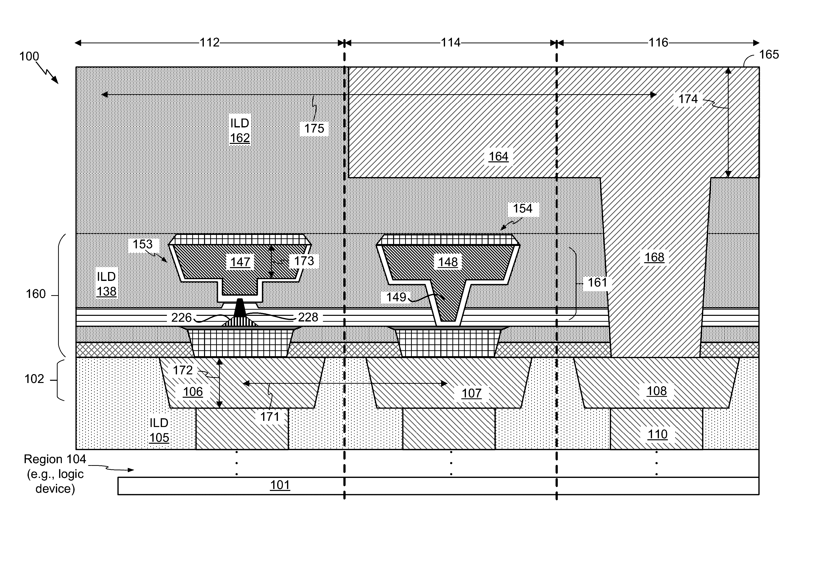
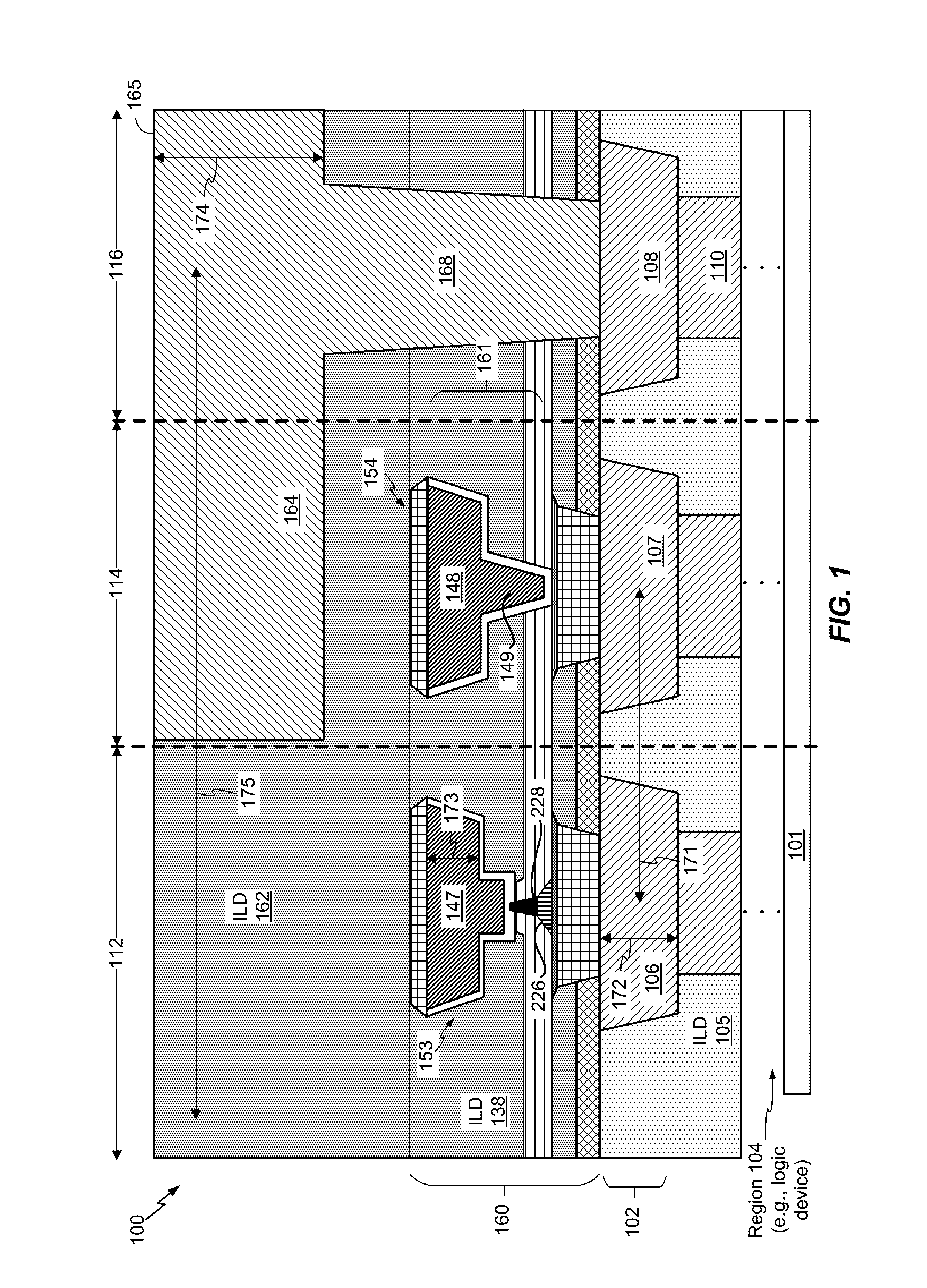
[0029]Referring to FIG. 1, a particular illustrative example of a device is depicted and generally designated 100. The device 100 may be included within an integrated circuit, such as a semiconductor die.

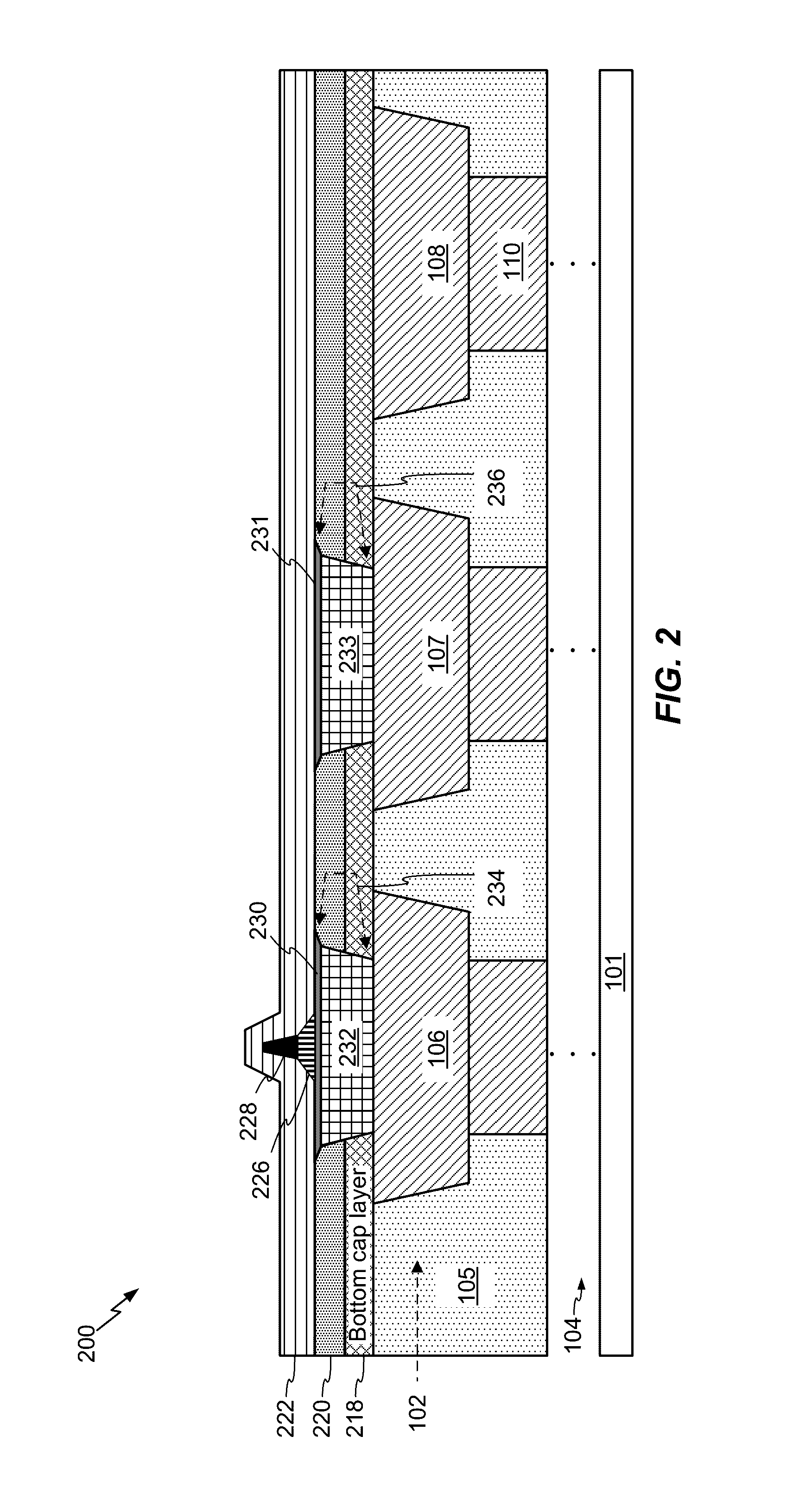
[0030]The device 100 includes a substrate 101, such as a silicon substrate. The device 100 further includes a region 104. The region 104 may include one or more devices formed using a plurality of layers of the device 100. For example, the region 104 may include a logic device (e.g., a processor, or another device) that is formed using a complementary metal-oxide-semiconductor (CMOS) logic process. The region 104 may further include wiring associated with the logic device. For example, the wiring may connect the logic device to the via 110.

[0031]The device 100 further includes one or more first structures formed using a plurality of metallization layers, such as a plurality of metallization layers associated with a back-end-of-line (BEOL) metallization process. To illustrate, FIG. 1...


PUM


Abstract

A method of fabrication of a device includes forming a first metallization layer that is coupled to a logic device of the device. The method further includes forming a second metallization layer that is coupled to a magnetoresistive random access memory (MRAM) module of the device. The second metallization layer is independent of the first metallization layer.

Description

I. FIELD[0001]This disclosure is generally related to semiconductor devices and more particularly to semiconductor devices that include memory devices.II. DESCRIPTION OF RELATED ART[0002]Magnetoresistive random access memory (MRAM) devices may use resistance-based storage elements to store information. For example, a magnetic tunnel junction (MTJ) may be programed to have either a low resistance state to indicate a first logic value (e.g., a logic zero value) or a high resistance state to indicate a second logic value (e.g., a logic one value).[0003]Some semiconductor devices integrate an MRAM device with one or more other components in a single integrated circuit. For example, an integrated circuit may include a substrate, a device formed on the substrate, and an MRAM device formed above the device using metallization layers of the integrated circuit. In this example, the MRAM device and the device may “share” the metallization layers. For example, the metallization layers may incl...

Claims


Application Information

Patent Timeline
Patent Type & Authority Applications(United States)
IPC IPC(8): H01L27/22H01L43/02H01L23/522G06F17/50H01L23/528H01L43/12H01L43/08
CPCH01L27/222H01L43/12H01L43/02H01L23/5226G06F17/5045H01L23/528H01L43/08H10B61/00H10N50/01H10N50/80H10N50/10H10N50/85G06F30/30
Inventor LU, YUKANG, SEUNG HYUK
Owner QUALCOMM INC
Why Eureka
Try Eureka