Display device and electronic apparatus including display device

a display device and electronic equipment technology, applied in the direction of electric digital data processing, instruments, computing, etc., can solve the problems of deteriorating sensing accuracy of optical sensors, difficult to dispose optical sensors in an inner side relative to the driving circuit, and easy influence of optical sensors, so as to prevent the increase of the fabrication cost of the liquid crystal display device, the detection accuracy is improved, and the accuracy is high.

Inactive Publication Date: 2008-11-13
JAPAN DISPLAY WEST
View PDF13 Cites 13 Cited by
  • Summary
  • Abstract
  • Description
  • Claims
  • Application Information

AI Technical Summary

Benefits of technology

[0013]The display device may further include a plurality of detection circuits, and a majority determination circuit connected to the plurality of detection circuits. The majority determination circuit changes an output signal when at least two of a plurality of results of detections output from the plurality of determination circuits are changed. With this configuration, when a shadow of a finger is formed on one of the plurality of sides or when a spotlight having a light intensity higher than external light encounters the one of the plurality of sides, a result of detection of the light intensity of the one of the plurality of sides is eliminated. Accordingly, the detection accuracy is improved. Furthermore, the plurality of detection circuits may include a first and a second detection circuits. Among the plurality of sub regions, sub regions connected to the first detection circuit among the plurality of detection circuits through the sensor lines may be arranged on one of the plurality of sides of the active matrix circuit, and sub regions connected to the second detection circuits among the plurality of detection circuits through the sensor lines may be arranged on one of the other remaining sides of the active matrix circuit. With this configuration, since a majority determination process is performed for the plurality of sides, even if a shadow is formed on a specific one of the plurality of sides or even if light having a high intensity is incident on a specific one of the plurality of sides, malfunction does not occur. Accordingly, external light is detected with high accuracy.
[0014]Moreover, the optical sensors may be PIN junction diodes or PN junction diodes formed of polysilicon thin films, and the driving circuits may include polysilicon thin film transistors. With this configuration, since the optical sensors and the thin-film transistors are formed in an identical fabrication process, the fabrication cost of the liquid crystal display device is prevented from increasing even when the optical sensors are incorporated in the liquid crystal display device.
[0015]According to another embodiment of the invention, there is provided an electronic apparatus including the display device. Since optical sensors having high detection accuracies are incorporated in the display device, an intensity of backlight can be readily controlled in accordance with external light. Accordingly, power consumption and fabrication cost is prevent from increasing. Furthermore, since photosensors may be arranged near a display region, the versatility of design features is improved.

Problems solved by technology

However, in a liquid crystal display device incorporating a driving circuit, it is difficult to dispose the optical sensors in an inner side relative to the driving circuit.
Furthermore, when the optical sensor is disposed near the display region, the optical sensors are likely to be influenced by electrical noise generated by driving the display region, and are likely to be influenced by stray light emitted from the display region.
Therefore, there arises a problem in that sensing accuracy of the optical sensor is deteriorated.
This problem is remarkable for the liquid crystal display device which performs common potential inversion driving.
Consequently, deterioration of accuracy of the detection caused by change of the potentials of the sensor lines due to electromagnetic noise generated by inversely driving the common electrode and coupling capacitance regarding the common electrode.

Method used


Image

  • Display device and electronic apparatus including display device
  • Display device and electronic apparatus including display device
  • Display device and electronic apparatus including display device

Examples


first embodiment

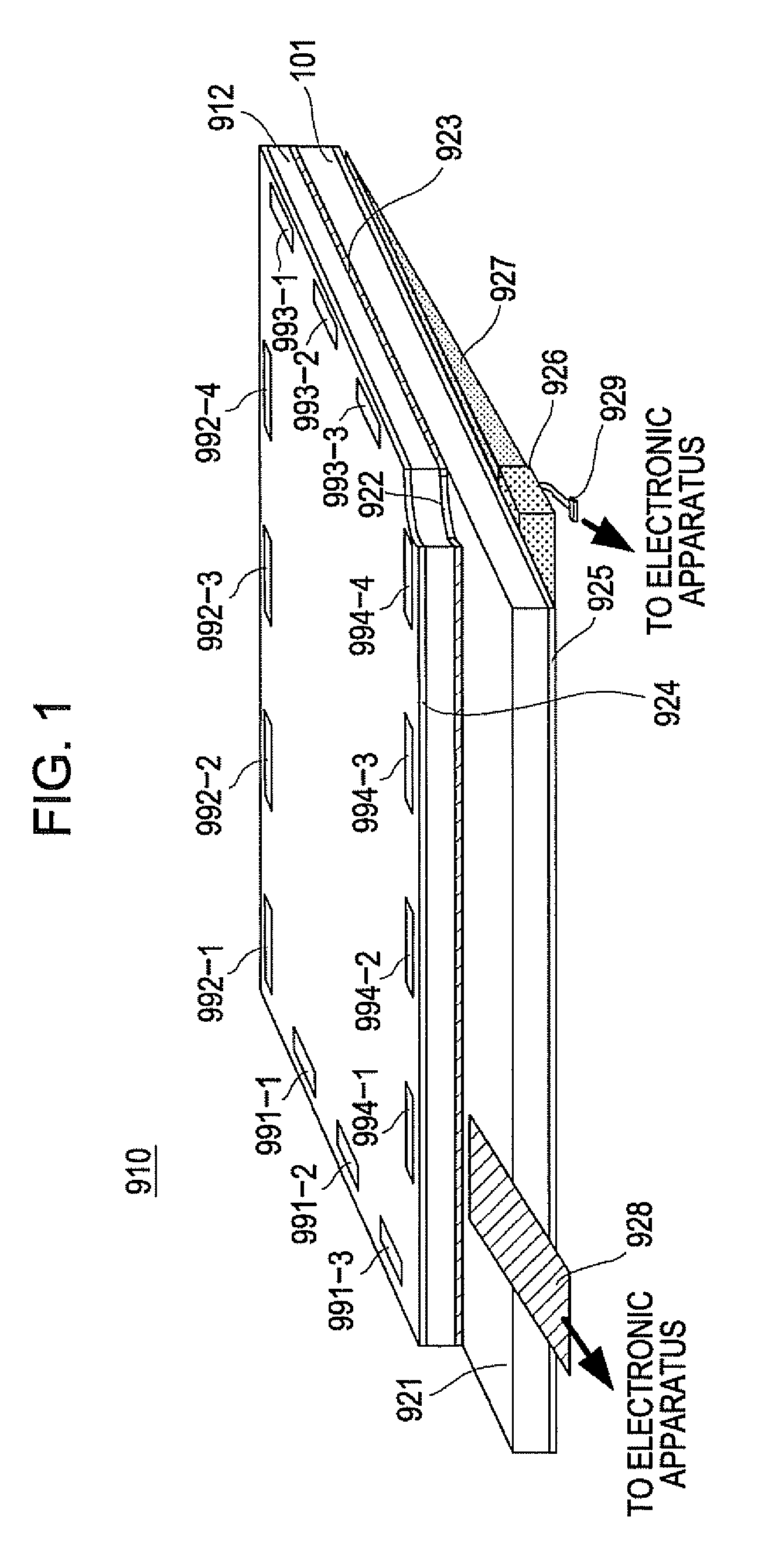
[0040]FIG. 1 is a perspective view (partial sectional view) illustrating a liquid crystal display device 910 according to a first embodiment of the present invention. The liquid crystal display device 910 includes an active matrix substrate 101, a counter substrate 912 attached to the active matrix substrate 101 using a seal member 923 with a predetermined gap therebetween, and nematic-phase liquid crystal material 922 interposed between the active matrix substrate 101 and the counter substrate 912. Furthermore, although not shown, alignment material formed of polyimide, for example, is applied onto the active matrix substrate 101 and is subjected to rubbing processing so as to obtain an alignment film on the active matrix substrate 101. The counter substrate 912 includes color filters (not shown) corresponding to pixels, a black matrix 940 (refer to FIG. 6, for example) which is formed of resin having a low reflection characteristic and low transmissivity which prevents light from ...

second embodiment

[0084]FIG. 16 is an enlarged plan view illustrating an n-th first-side optical sensor 351-n included in a first-side light-receiving sensor group according to a second embodiment, and corresponds to the n-th first-side optical sensor 351-n according to the first embodiment shown in FIG. 8. The explanatory note shown in FIG. 5 is also employed in FIG. 16. Different points between the n-th first-side optical sensor 351-n shown in FIG. 16 and the n-th first-side optical sensor 351-n shown in FIG. 8 are mainly described hereinafter.

[0085]Unlike the scanning line 201-n shown in FIG. 8, a scanning line 201-n shown in FIG. 16 is formed of a thin film of an alloy of aluminum and neodymium (AlNd) through a contact hole in a region overlapped with a light-shielding electrode 611-n in a plan view. A common potential branch line 618-n formed of a molybdenum (Mo) thin film is arranged between the scanning line 201-n and the light-shielding electrode 611-n. The common potential branch line 618-n ...

third embodiment

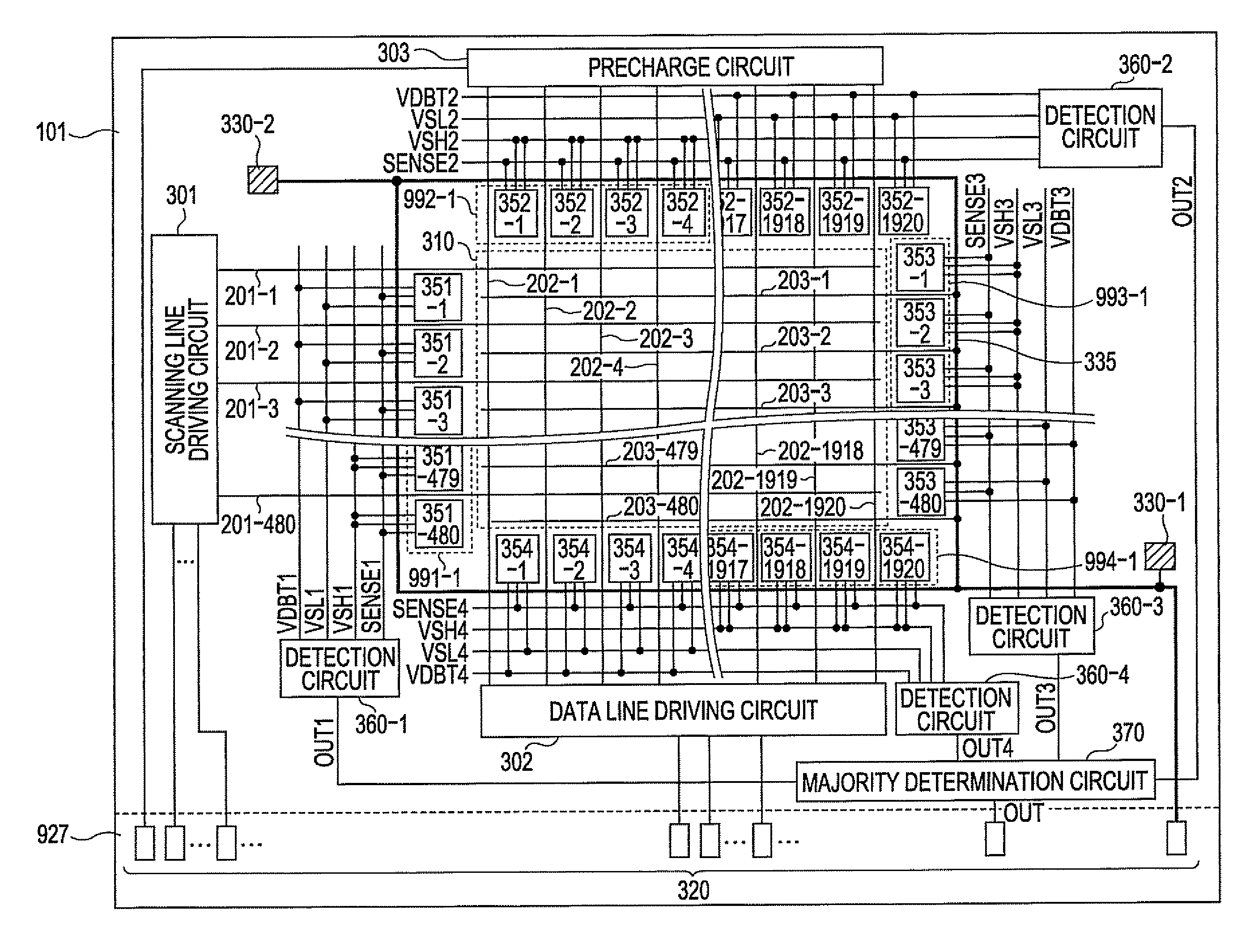
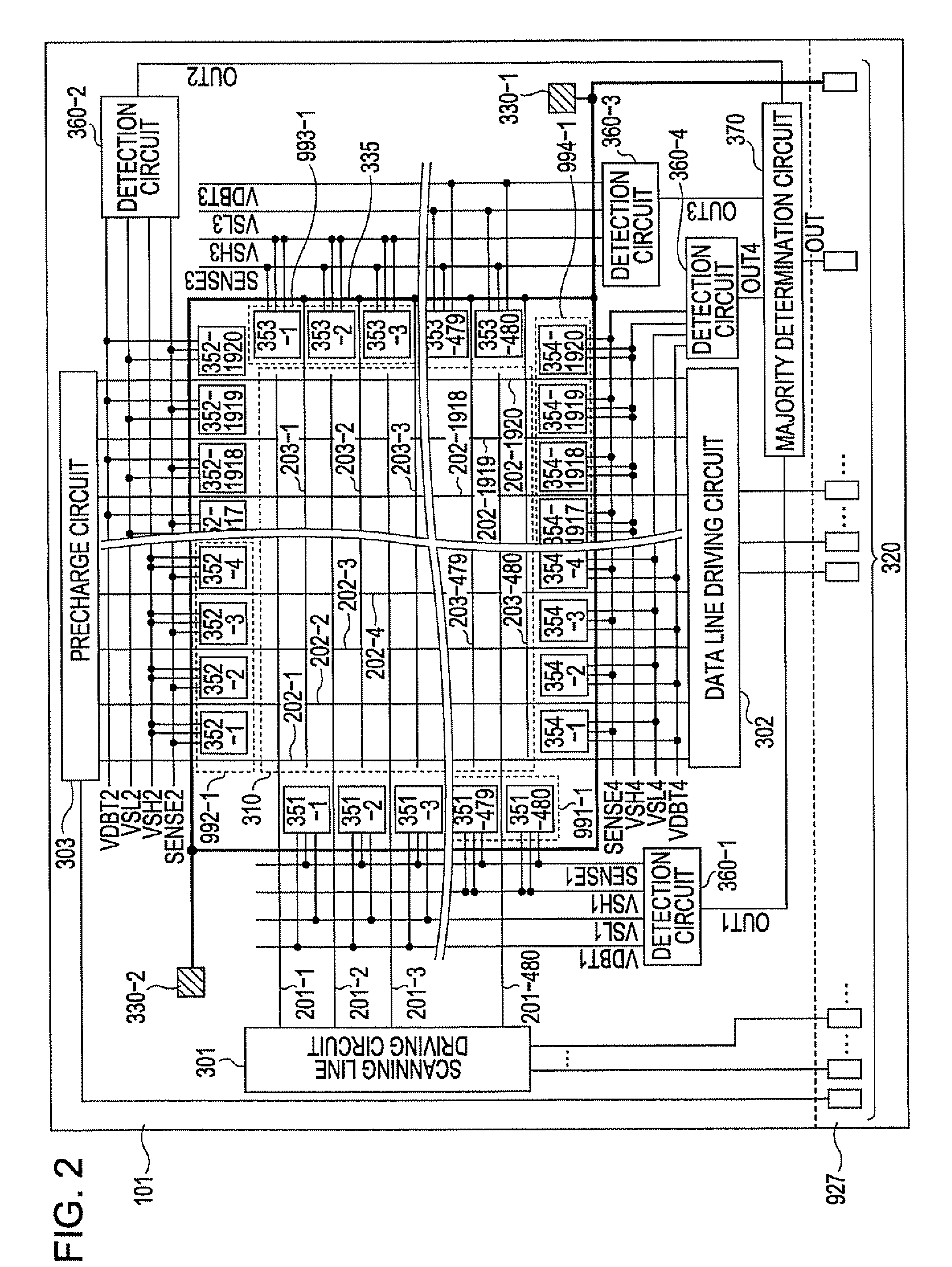
[0091]FIG. 18 is a diagram illustrating a configuration of an active matrix substrate 102 according to a third embodiment. Different points between the active matrix substrate 102 and the active matrix substrate 101 according to the first embodiment shown in FIG. 2 are mainly described hereinafter. Components shown in FIG. 18 similar to those shown in FIG. 2 are denoted by the reference numerals used in FIG. 2 and descriptions thereof are omitted. In this embodiment, first-side optical sensors 351′-1 to 351′-480 are arranged as optical sensors 351′ instead of the first-side optical sensors 351-1 to 351-480 of the first embodiment, second-side optical sensors 352′-1 to 352′-1920 are arranged as optical sensors 352′ instead of the second-side optical sensors 352-1 to 352-1920, third-side optical sensors 353′-1 to 353′-480 are arranged as optical sensors 353′ instead of the third-side optical sensors 353-1 to 353-480, and fourth-side optical sensors 354′-l to 354′-1920 are arranged as ...


PUM

PropertyMeasurementUnit
voltagesaaaaaaaaaa
thicknessaaaaaaaaaa
thicknessaaaaaaaaaa

Abstract

A display device includes an active matrix circuit for display, a plurality of bus lines which are connected to the active matrix circuit and which are used to transmit driving signals, driving circuits which supply the driving signals to the plurality of bus lines, the plurality of bus lines and the driving circuits being arranged on a substrate, and optical sensors arranged on the substrate. The optical sensors are arranged in a plurality of sub regions separated using the plurality of bus lines. The plurality of sub regions are arranged between the active matrix circuit and each of the driving circuits.

Description

BACKGROUND[0001]1. Technical Field[0002]The present invention relates to a display device and an electronic apparatus including the display device.[0003]2. Related Art[0004]In recent years, a technique of incorporating an optical sensing function in a liquid crystal display device employing a thin film transistor, in particular, has been developed (refer to Japanese Unexamined Patent Application Publication No. 2006-118965, for example) in order to obtain the following advantages using optical sensors. (1) Power consumption is reduced and image quality is improved by controlling luminance, for example, by measuring external light. (2) The luminance and chromaticity is controlled by measuring backlight. (3) The optical sensors are used as a touch key so as to detect a position of a finger or a light pen. Examples of the optical sensors include thin-film transistors, PIN (p-intrinsic-n) diodes, and PN diodes. The optical sensors preferably have light-receiving sections formed of silic...

Claims


Application Information

Patent Timeline
Patent Type & Authority Applications(United States)
IPC IPC(8): G06F3/042G02F1/133
CPCG02F1/13318G09G3/3406G09G3/3614G09G3/3648G09G2360/144
Inventor KOBASHI, YUTAKA
Owner JAPAN DISPLAY WEST
Why Eureka
Try Eureka