FORMATION OF SiN THIN FILMS

Active Publication Date: 2017-03-02
ASM IP HLDG BV
View PDF5 Cites 328 Cited by
  • Summary
  • Abstract
  • Description
  • Claims
  • Application Information

AI Technical Summary

Benefits of technology

[0021]In some embodiments, the hydrogen-containing gas and the nitrogen-containing gas are used to form the nitrogen-containing plasma. In some embodi

Problems solved by technology
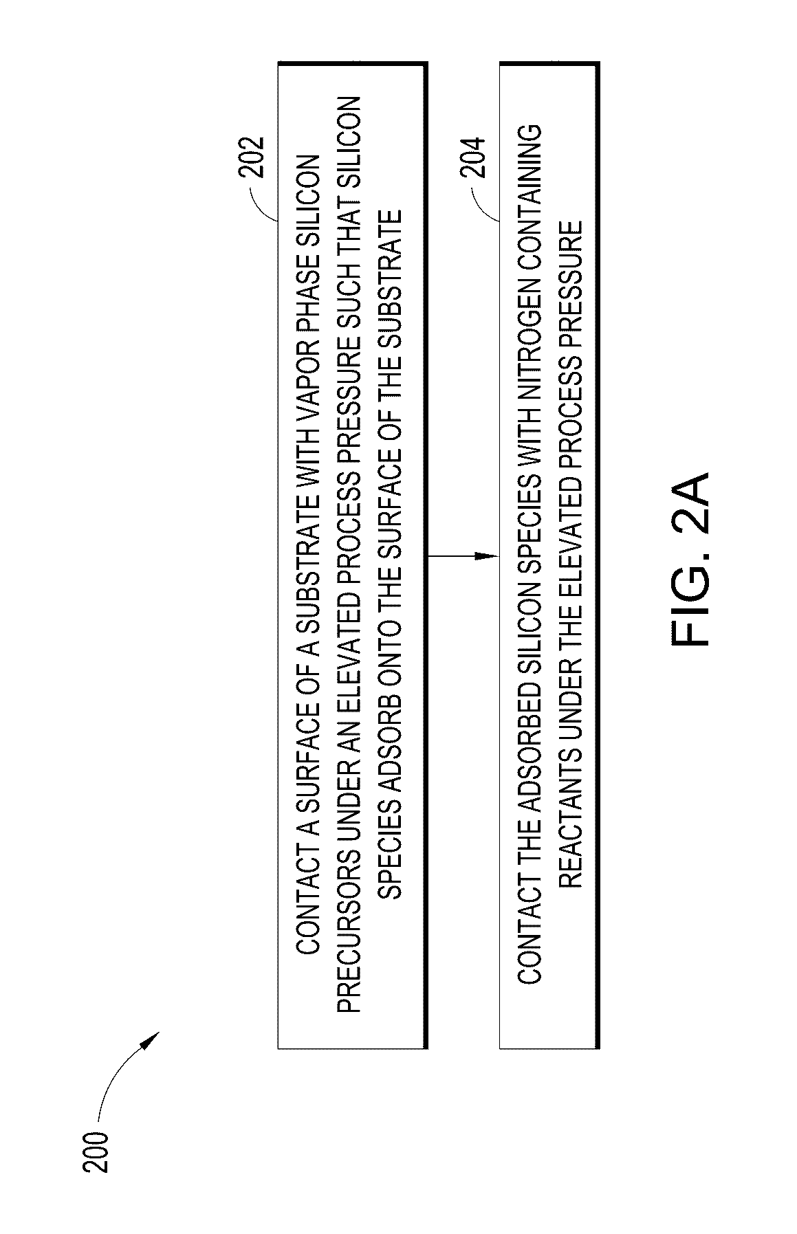
Current PEALD silicon nitride processes in general suffer from anisotropic etch behavior when used to deposit on a three-dimensional structure, such as a trench structure.
In other words, the film deposited on the sidewalls of a trench or

Method used


Image

  • FORMATION OF SiN THIN FILMS
  • FORMATION OF SiN THIN FILMS
  • FORMATION OF SiN THIN FILMS

Examples


Embodiment Construction

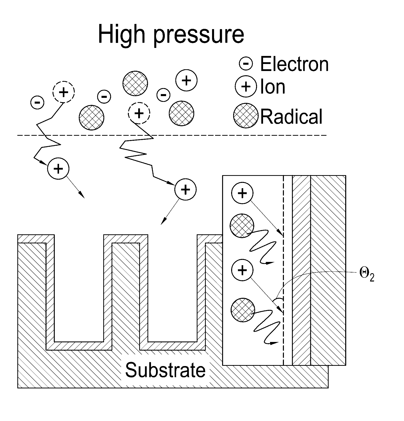
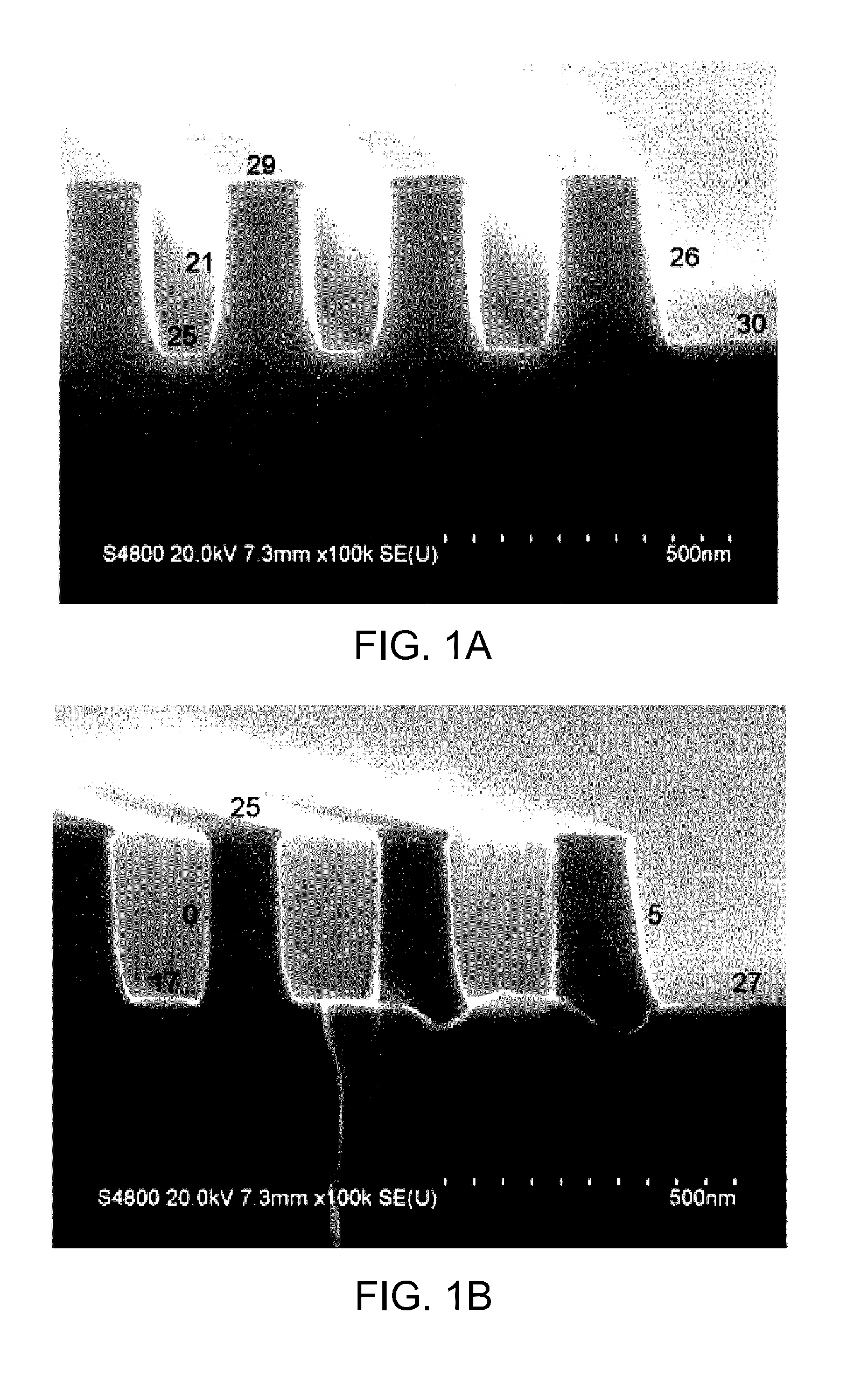
[0030]Silicon nitride films have a wide variety of applications, as will be apparent to the skilled artisan, such as in planar logic, DRAM, and NAND Flash devices. More specifically, conformal silicon nitride thin films that display uniform etch behavior have a wide variety of applications, both in the semiconductor industry and also outside of the semiconductor industry. According to some embodiments of the present disclosure, various silicon nitride films and precursors and methods for depositing those films by atomic layer deposition (ALD) are provided. Importantly, in some embodiments the silicon nitride films have a relatively uniform etch rate for both vertical and horizontal portions, when deposited onto 3-dimensional structures. Such three-dimensional structures may include, for example and without limitation, FinFETS or other types of multiple gate FETs. In some embodiments, various silicon nitride films of the present disclosure have an etch rate of less than half the ther...


PUM

PropertyMeasurementUnit
Temperatureaaaaaaaaaa
Percent by massaaaaaaaaaa

Abstract

Methods of forming silicon nitride thin films on a substrate in a reaction space under high pressure are provided. The methods can include a plurality of plasma enhanced atomic layer deposition (PEALD) cycles, where at least one PEALD deposition cycle comprises contacting the substrate with a nitrogen plasma at a process pressure of 20 Torr to 500 Torr within the reaction space. In some embodiments the silicon precursor is a silyly halide, such as H2SiI2. In some embodiments the processes allow for the deposition of silicon nitride films having improved properties on three dimensional structures. For example, such silicon nitride films can have a ratio of wet etch rates on the top surfaces to the sidewall of about 1:1 in dilute HF.

Description

BACKGROUND[0001]Field[0002]The present disclosure relates generally to the field of semiconductor device manufacturing and, more particularly, to low temperature formation of silicon nitride thin films.[0003]Description of the Related Art[0004]Spacers are widely used in semiconductor manufacturing as structures to protect against subsequent processing steps. For example, nitride spacers formed beside gate electrodes can be used as a mask to protect underlying source / drain areas during doping or implanting steps.[0005]As the physical geometry of semiconductor devices shrinks, the gate electrode spacer becomes smaller and smaller. The spacer width is limited by the nitride thickness that can be deposited conformably over the dense gate electrodes lines. Thus, the nitride spacer etching process is preferred to have a high ratio of spacer width to nitride layer thickness as deposited.[0006]Current PEALD silicon nitride processes in general suffer from anisotropic etch behavior when used...

Claims


Application Information

Patent Timeline
IPC IPC(8): H01L21/02
CPCH01L21/0228H01L21/02208H01L21/02274H01L21/0217C23C16/45542C23C16/045C23C16/345H01L21/02219H01L21/02211C23C16/45553
Inventor SUZUKI, TOSHIYAPORE, VILJAMI J.CHEN, SHANGYAMADA, RYOKOISHIKAWA, DAINAMBA, KUNITOSHI
Owner ASM IP HLDG BV
Why Eureka
Try Eureka