Shielding structure for integrated inductor/transformer

Active Publication Date: 2017-03-16
REALTEK SEMICON CORP
View PDF7 Cites 9 Cited by
  • Summary
  • Abstract
  • Description
  • Claims
  • Application Information

AI Technical Summary

Benefits of technology

[0009]To sum up, in the shielding structures for integrated inductors/transformers disclosed by the present disclosure, the surrounding of the shielding structure is not closed but has openings, and the center of the shielding structure is not hollow because the conductive units are connected at the center of the shielding structure. In this manner, the Eddy current effect can be reduced so as to prevent the reverse magnetic field formed by the induced current from damaging the integrated inductor/transformer. Thus, the characteristics of the integrated inductor/tr

Problems solved by technology

Generally, integrated inductors or transformers are configured on a silicon substrate, so when the entire integrated circuit is working the silicon substrate may be coupled with a generated electromagnetic energy, which causes substrate losses and makes the Q factor (the Quality factor, which is the ratio of the power storage and the power consumption) drop.
In this case, when the inductor or the transforme

Method used


Image

  • Shielding structure for integrated inductor/transformer
  • Shielding structure for integrated inductor/transformer
  • Shielding structure for integrated inductor/transformer

Examples


Embodiment Construction

[0022]The aforementioned illustrations and following detailed descriptions are exemplary for the purpose of further explaining the scope of the present disclosure. Other objectives and advantages related to the present disclosure will be illustrated in the subsequent descriptions and appended drawings.

[0023]It will be understood that, although the terms first, second, third, and the like, may be used herein to describe various elements, but these elements should not be limited by these terms. These terms are only to distinguish one element, region or section from another element, region or section. Thus, a first element, region or section discussed below could be termed a second element, region or section without departing from the teachings of the present disclosure. As used herein, the term “and / or” includes any and all combinations of one or more of the associated listed items.

One Embodiment of the Shielding Structure

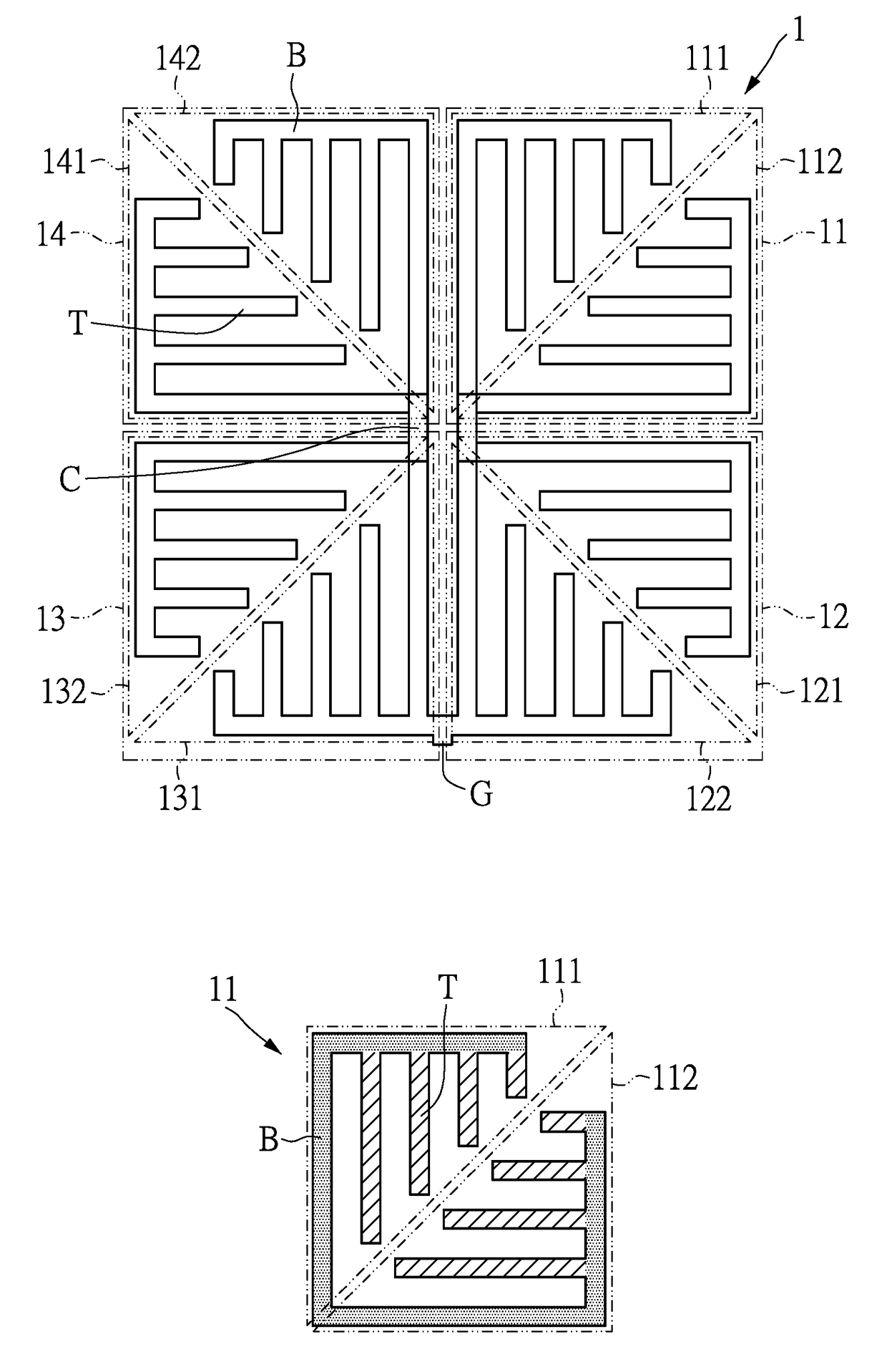
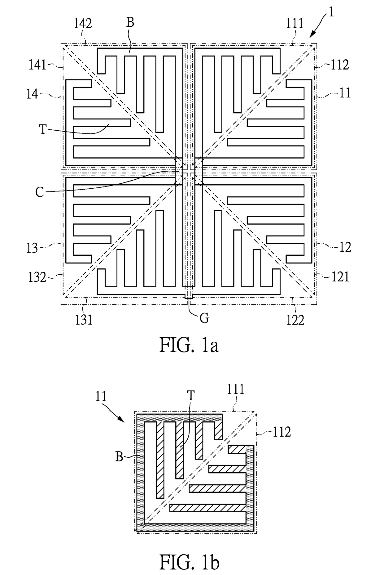
[0024]Referring to FIG. 1a and FIG. 1b, FIG. 1a shows a schemat...


PUM


Abstract

Disclosed is a shielding structure for an integrated inductor/transformer, configured under the integrated inductor or the transformer and upon a substrate. The shielding structure comprises conductive units, first connecting portions, via holes, a second connecting portion and a grounding portion. Each conductive unit comprises a first conductive portion and second conductive portions extending from the first conductive portion. The number of the second conductive portions is odd. The length of each second conductive portion progressively diminishes from a center of the first conductive portion to both of two ends of the first conductive portion. The first connecting portion connects the first conductive portions of the conductive units through via holes. The grounding portion is connected to one of the first conductive portions. The second connecting portion connects all longest second conductive portions together. Moreover, the conductive units and the second connecting portion are made of different conductive materials.

Description

BACKGROUND OF THE INVENTION[0001]1. Field of the Invention[0002]The present disclosure relates to a shielding structure; in particular, to a shielding structure for integrated inductors / transformers.[0003]2. Description of Related Art[0004]Generally, integrated inductors or transformers are configured on a silicon substrate, so when the entire integrated circuit is working the silicon substrate may be coupled with a generated electromagnetic energy, which causes substrate losses and makes the Q factor (the Quality factor, which is the ratio of the power storage and the power consumption) drop. Under two ideal circumstances, substrate losses can almost be prevented. In one, the silicon substrate has an infinitely great resistance, and in the other, the silicon substrate has barely resistance. However, the resistance of the silicon substrate is commonly 10˜15 Ohm-Cm. In this case, when the inductor or the transformer is working at a high frequency, there will be a coupling current gen...

Claims


Application Information

Patent Timeline
IPC IPC(8): H01F27/36H05K1/02H05K1/11H01F27/34
CPCH01F27/36H01F27/34H01F2027/348H05K1/115H05K1/0218H01F27/363H05K9/0064
Inventor HUANG, KAI-YIYEN, HSIAO-TSUNGCHEN, TAI-SHENG
Owner REALTEK SEMICON CORP
Why Eureka
Try Eureka