Manufacture method of amoled back plate and structure thereof

Active Publication Date: 2017-03-16
TCL CHINA STAR OPTOELECTRONICS TECH CO LTD
View PDF6 Cites 3 Cited by
  • Summary
  • Abstract
  • Description
  • Claims
  • Application Information

AI Technical Summary

Benefits of technology

[0047]The benefits of the present invention are as follows. The present invention provides a manufacture method of an AMOLED back plate, in which by deposing and patterning a P type heavy doped micro silicon layer to form a source/a drain, and making the source/the drain and a gate be mutually spaced in a horizontal direction, the contact resistance between the source/the drain and a first poly-silicon section can be reduced to improve the electrical property of a drive TFT to make a conductive current higher and a leakage current lower, and diminish image sticking for raisin

Problems solved by technology

In addition, the source/the drain 401 and the gate 601 partially overlap each other in the hor

Method used


Image

  • Manufacture method of amoled back plate and structure thereof
  • Manufacture method of amoled back plate and structure thereof
  • Manufacture method of amoled back plate and structure thereof

Examples


Embodiment Construction

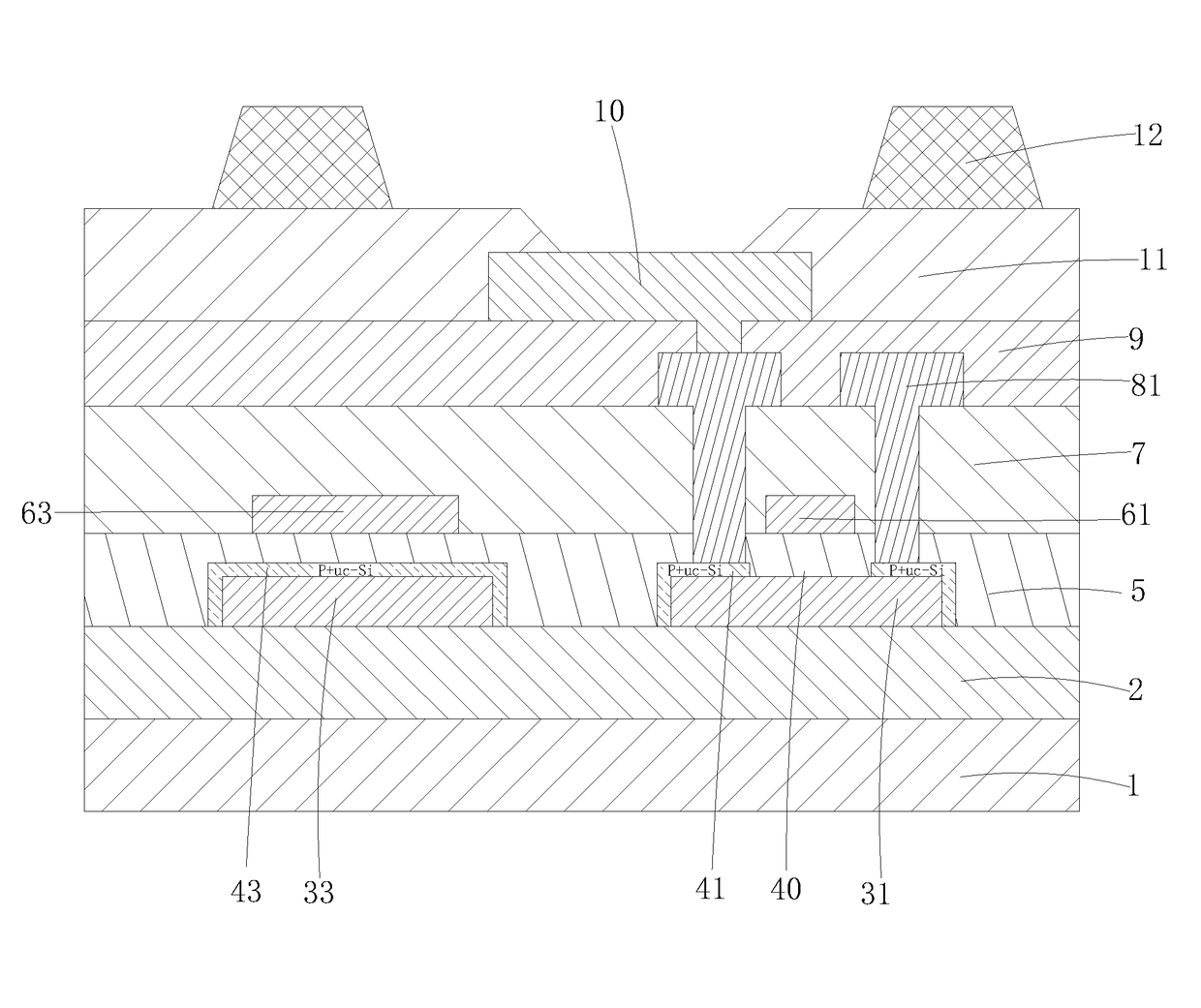
[0057]For better explaining the technical solution and the effect of the present invention, the present invention will be further described in detail with the accompanying drawings and the specific embodiments.

[0058]Referring to FIGS. 2-7, the present invention provides a manufacture method of an AMOLED back plate, comprising the following steps:

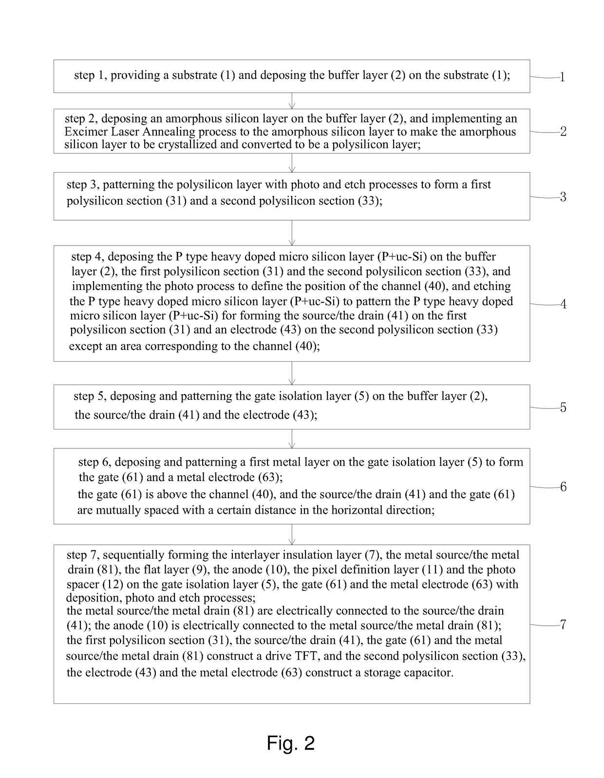
[0059]step 1, providing a substrate 1 and deposing a buffer layer 2 on the substrate 1.

[0060]The substrate 1 is a transparent substrate. Preferably, the substrate 1 is a glass substrate or a plastic substrate.

[0061]A material of the buffer layer 2 is silicon nitride (SiNx), silicon oxide (SiOx), or a combination thereof.

[0062]step 2, deposing an amorphous silicon layer on the buffer layer 2, and implementing an excimer laser annealing process to the amorphous silicon layer to make the amorphous silicon layer crystallized and converted into a poly-silicon layer.

[0063]step 3, as shown in FIG. 3, patterning the poly-silicon layer with photo and...


PUM


Abstract

An AMOLED back plate includes a substrate on which a buffer layer and a poly-silicon section are sequentially formed. A source and a drain are respectively formed of P-type heavy doped micro silicon on the poly-silicon section that have edges facing and spaced from each other to define a channel therebetween. A gate isolation layer is formed on the buffer layer, the source, the drain and the channel. A gate is formed on the gate isolation layer and has opposite edges that face in directions toward the edges of the source and the drain. The opposite edges of the gate are spaced from the edges of the source and the drain by predetermined spacing distance in horizontal directions so as to prevent the gate from overlapping the source and the drain.

Description

CROSS REFERENCE TO RELATED APPLICATIONS[0001]This is a divisional application of co-pending U.S. patent application Ser. No. 14 / 429,082, filed on Mar. 18, 2015.BACKGROUND OF THE INVENTION[0002]1. Field of the Invention[0003]The present invention relates to a display technology field, and more particularly to a manufacture method of an AMOLED back plate and a structure thereof.[0004]2. The Related Arts[0005]In the display field, liquid crystal display (LCD), organic light emitting diode (OLED) and other panel display techniques have been gradually replaced the conventional cathode ray tube (CRT) displays. The OLED possesses many outstanding properties of self-illumination, low driving voltage, high luminescence efficiency, fast response, high clarity and contrast, near 180° view angle, wide range of working temperature, applicability of flexible display and large scale full color display. The OLED is considered as the most potential flat panel display technology.[0006]The OLED can be...

Claims


Application Information

Patent Timeline
IPC IPC(8): H01L27/32H01L51/52
CPCH01L27/3262H01L2251/301H01L27/3246H01L27/3248H01L51/5215H01L29/78603H01L29/78675H01L29/78696H01L29/7833H01L27/1222H01L27/1255H01L27/1274H01L29/4908H01L2227/323H01L2251/308H01L27/3265H01L29/458H01L29/66757H10K59/1213H10K50/816H10K59/122H10K59/123H10K59/1216H10K71/00H10K59/1201H10K2102/00H10K2102/102H10K2102/103H01L21/02532H01L21/02592H01L21/0262H01L21/02675H01L21/30604H01L29/41775H01L29/4958
Inventor HSU, YUANJUN
Owner TCL CHINA STAR OPTOELECTRONICS TECH CO LTD
Why Eureka
Try Eureka