Method and apparatus for drying semiconductor substrates using liquid carbon dioxide

a technology of liquid carbon dioxide and semiconductor substrates, which is applied in lighting and heating apparatus, cleaning using liquids, and inorganic non-surface active detergent compositions, etc. it can solve the problems of contaminating the process and reducing the processing efficiency of semiconductor substrates, so as to reduce the processing temperature and pressure, reduce the processing cost, and reduce the effect of processing tim

Inactive Publication Date: 2017-03-30
TOKYO ELECTRON LTD
View PDF7 Cites 4 Cited by
  • Summary
  • Abstract
  • Description
  • Claims
  • Application Information

AI Technical Summary

Benefits of technology

[0010]The low processing temperature and pressure required for Liq-CO2 processing provides a wider process latitude compared to other solutions, including sc-CO2. Moreover, this invention alleviates the requirements on the processing equipment such as pumps, gaskets, fittings, piping, chamber material, welding, and other items, with a significant equipment fabrication cost reduction. The operation point of pressure and temperature of the Liq-CO2 process also significantly reduce chamber and equipmen

Problems solved by technology

With the scaling of dimensions on the semiconductor integrated circuits, as is known the forces exerted based on surface tension and contact angle on the features present on the semiconductor surface during the drying process have increased and, if non-optimized drying processes are used,

Method used


Image

  • Method and apparatus for drying semiconductor substrates using liquid carbon dioxide
  • Method and apparatus for drying semiconductor substrates using liquid carbon dioxide

Examples


Embodiment Construction

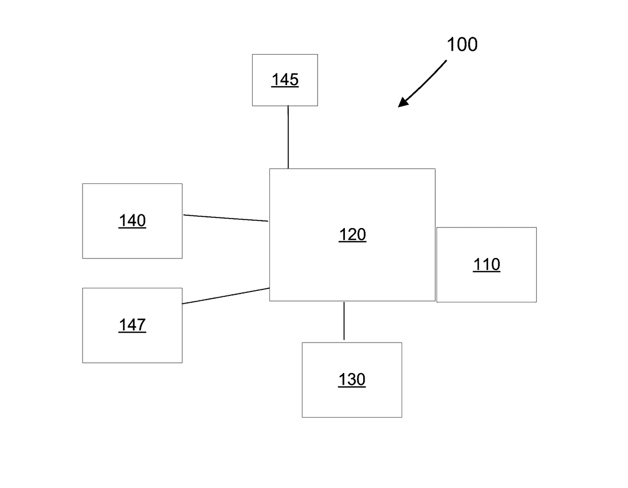
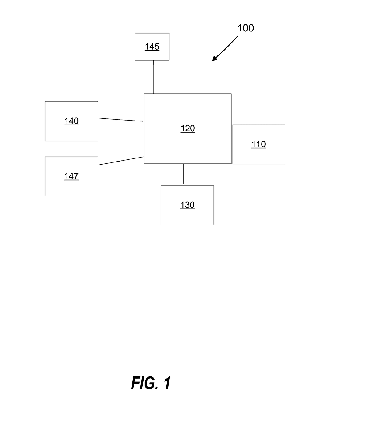
[0015]A drying method for a semiconductor substrate, in accordance with an embodiment of the invention is described herein. In this regard, a semiconductor substrate is treated with a chemical solution; the semiconductor substrate is rinsed with deionized water (DIW); the liquid covering a surface of the semiconductor substrate is changed from the deionized water to a water soluble organic solvent (i.e. Isopropyl alcohol—IPA) by for example displacing the water with the IPA, the semiconductor substrate wet with the water soluble organic solvent is transferred to a drying chamber; the water soluble organic solvent on the semiconductor substrate is rinsed with liquid carbon dioxide; and the liquid carbon dioxide and the alcohol is discharged from the drying chamber.

[0016]Alternatively, the step which includes use of a water soluble organic solvent can be eliminated and the semiconductor substrate is transferred wet with DIW to the drying chamber, and subsequently the DIW is rinsed (su...


PUM


Abstract

Method and apparatus for rinsing and drying a semiconductor substrate having a first rinse liquid such as water on the substrate in a substrate processing system. The method includes dispensing onto the substrate liquid carbon dioxide to displace any liquid present on the substrate and to dry the substrate. The apparatus includes a chamber for rinsing and drying the substrate.

Description

[0001]This application claims priority to U.S. provisional application Ser. No. 62 / 235,126, filed Sep. 30, 2015, incorporated by reference in its entirety.TECHNICAL FIELD OF THE INVENTION[0002]This invention relates to wet treatment of semiconductor surfaces. More specifically, it provides a novel method for drying semiconductor surfaces, an apparatus for implementing the proposed method, and related methods.BACKGROUND[0003]Drying of a semiconductor surface involves the removal of water, an aqueous solution, a solvent, an organic solution, any other processing liquid that was used to treat the semiconductor surface, or any mixture of two or more thereof. The drying process should result in a pristine semiconductor surface free of the processing liquid without damaging any of the surface features. Supercritical carbon dioxide (sc-CO2) has been proposed for use in drying semiconductor surfaces. In such processes, for example, water on a substrate is displaced with isopropyl alcohol, t...

Claims


Application Information

Patent Timeline
IPC IPC(8): H01L21/02B08B3/10C11D11/00H01L21/687H01L21/67C11D7/04B08B3/08H01L21/324
CPCH01L21/02057B08B3/08B08B3/102C11D11/0047H01L21/68764H01L21/67028C11D7/04H01L21/324F26B21/14F26B9/06H01L21/02046H01L21/02052H01L21/67034H01L21/6704
Inventor BROWN, IAN J.PRINTZ, WALLACE P.ROTONDARO, ANTONIO LUIS PACHECOGOSHI, GENTAROEGASHIRA, KEISUKE
Owner TOKYO ELECTRON LTD
Why Eureka
Try Eureka