
Photolithographic patterning of electronic devices

a technology of electronic devices and photolithography, applied in the direction of photomechanical devices, instruments, coatings, etc., can solve the problems of affecting the position accuracy of the mask opening, affecting the quality of the mask, etc., to achieve the effect of wide processing latitude, rapid processing, and easy lifting o

Active Publication Date: 2018-06-05
ORTHOGONAL
View PDF29 Cites 0 Cited by
  • Summary
  • Abstract
  • Description
  • Claims
  • Application Information

AI Technical Summary

Benefits of technology

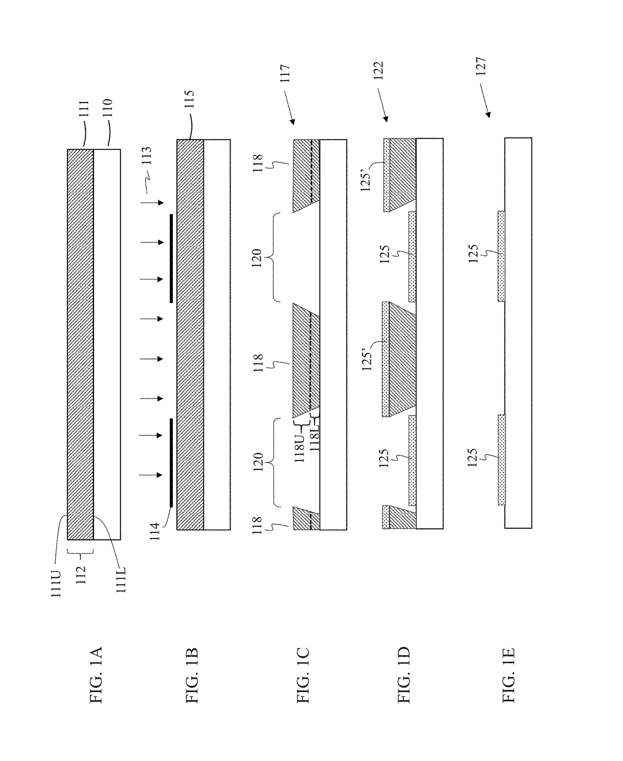
[0010]Methods and compositions disclosed herein can be used to form undercut photopolymer structures that are easily lifted off, thereby making them very useful for patterning devices. The methods and materials enable a wide processing latitude for making such structures. Fluorinated solvents and materials provide gentle processing conditions, compatible with organic electronic and bioelectronic devices. The rapid processing and low toxicity of the methods and materials make the disclosed systems also very useful for patterning non-organic electronic devices such as MEMS.

Problems solved by technology

A key challenge for full-color OLED displays is patterning the array of red, green and blue pixels.
However, a vapor deposited film builds up on the mask which may eventually narrow the mask openings or cause deforming stresses on the mask.
Therefore, it is necessary to clean the mask after a certain number of uses, which is disadvantageous from the viewpoint of manufacturing costs.
In addition, when a fine metal mask is increased in size to accommodate larger substrates, the positional accuracy of the mask openings becomes much more difficult, both from the standpoint of initial alignment and then maintaining the alignment during deposition due to thermal expansion issues.
Positional accuracy may be improved to a degree by enhancing the stiffness of a frame of the mask, but this increase the weight of the mask itself causes other handling difficulties.

Method used


Image

  • Photolithographic patterning of electronic devices
  • Photolithographic patterning of electronic devices
  • Photolithographic patterning of electronic devices

Examples


examples

Fluorinated Photopolymer Composition 1

[0182]A copolymer was prepared by copolymerizing FOMA (a first monomer having a fluorine-containing group), ECPMA (a second monomer having a solubility-altering reactive group), DBCMA shown below (a third monomer having a radiation-absorbing dye), and a branching monomer ethylene glycol dimethacrylate (“EGDMA”). Polymerization was carried out in the presence of 1-dodecanethiol (“DDT”) as a chain transfer agent and using 2,2′-azodi(2-methylbutyronitrile) (“AMBN”) as the radical chain initiator. The relative mole ratios of FOMA / ECPMA / DBCMA / EGDMA were 48 / 40 / 8 / 4 mol %, respectively, and the copolymer had a fluorine content of about 36.6% by weight. The following procedure was be used.

[0183]

[0184]A 100 mL flask was charged with 21.9 g HFE-6512 solvent, 6.0 g FOMA, 2.11 g ECPMA, 0.23 g EGDMA, 1.03 g DBCMA, 0.11 g AMBN, and 0.18 g DDT. The mixture was deaerated by sparging with nitrogen for 15 min, then sealed and placed in an oil bath at 70° C. The oi...


PUM

PropertyMeasurementUnit
thicknessaaaaaaaaaa
thicknessaaaaaaaaaa
thicknessaaaaaaaaaa

Abstract

A method of patterning a device includes forming a fluorinated photopolymer layer over a device substrate. The photopolymer layer has a lower portion proximate the device substrate and an upper portion distal the device substrate. The fluorinated photopolymer layer includes a radiation-absorbing dye and a fluorinated photopolymer having a solubility-altering reactive group. The photopolymer layer is exposed to patterned radiation to form exposed and unexposed areas in accordance with the patterned radiation and a developed structure is formed by removing unexposed areas using a developing agent that includes a first fluorinated solvent. The lower portion of the exposed area of the photopolymer layer has a dissolution rate in the developing agent that is at least 5 times higher than a dissolution rate for the upper portion.

Description

CROSS-REFERENCE TO RELATED APPLICATIONS[0001]This application is a Continuation-in-Part of PCT / US2015 / 000196, filed on Dec. 23, 2015 which claims the benefit of priority of U.S. Provisional Application No. 62 / 096,584, filed on Dec. 24, 2014 and which applications are incorporated herein by reference.BACKGROUND1. Field of the Disclosure[0002]The present disclosure relates to patterning of organic, electronic and organic electronic devices. The disclosed methods and materials are particularly useful for lift-off patterning, e.g., for forming OLED devices.2. Discussion of Related Art[0003]Organic electronic devices may offer significant performance and price advantages relative to conventional inorganic-based devices. As such, there has been much commercial interest in the use of organic materials in electronic device fabrication. For example, displays based on organic light-emitting diode (OLED) technology have recently gained popularity and offer numerous advantages over many other d...

Claims


Application Information

Patent Timeline
Patent Type & Authority Patents(United States)
IPC IPC(8): H01L21/00H01L51/00H01L21/027C08F214/18C09D4/00C08K3/16
CPCH01L21/0272C08F214/18H01L51/0011C09D4/00C08K3/16C08F222/10G03F7/0046G03F7/038G03F7/0388G03F7/0392G03F7/0397G03F7/325H10K71/166C08F220/00G03F7/004H10K71/233H10K71/00
Inventor ROBELLO, DOUGLAS ROBERTO'TOOLE, TERRENCE ROBERTBYRNE, FRANK XAVIERFREEMAN, DIANE CAROLWRIGHT, CHARLES WARRENRUBSAM, SANDRABOBLAK, KENNETH NICHOLASZHAO, MENG
Owner ORTHOGONAL
Learn More