

Photolithographic patterning of electronic devices
Patent Information
- Authority / Receiving Office
- US · United States
- Patent Type
- Applications(United States)
- Current Assignee / Owner
- ORTHOGONAL
- Publication Date
- 2017-10-05
Smart Images
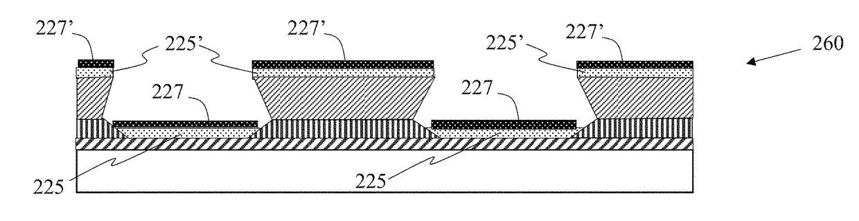
Figure 1 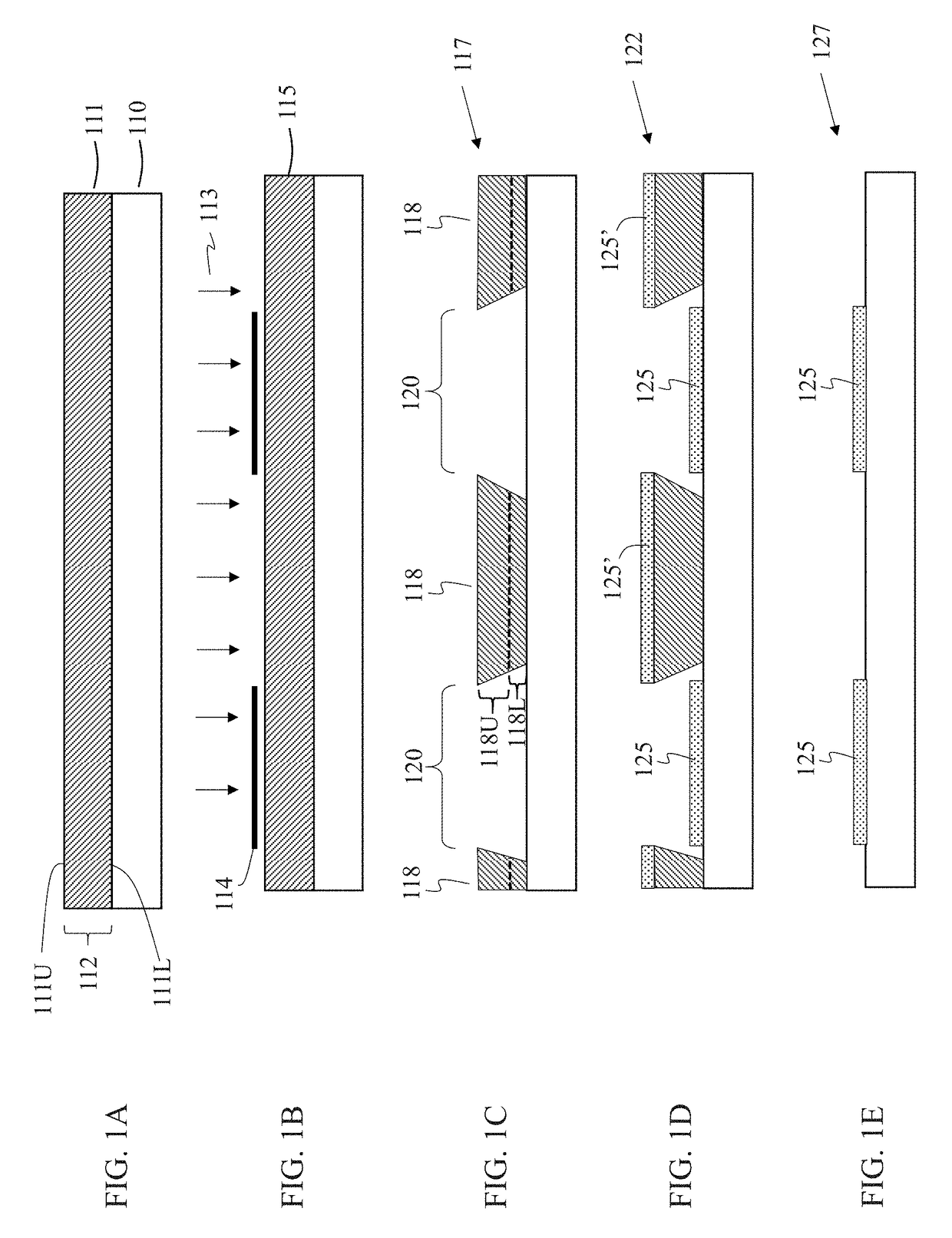
Figure 2 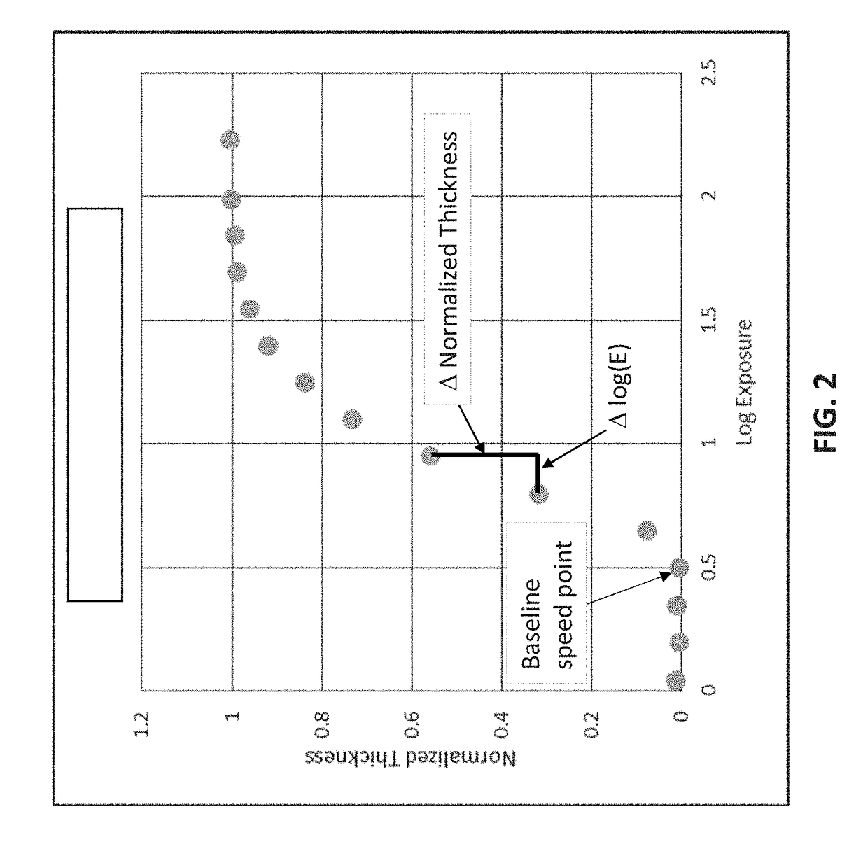
Figure 3
Abstract
Description
CROSS-REFERENCE TO RELATED APPLICATIONS
[0001] This application is a Continuation-in-Part of PCT / US2015 / 000196, filed on Dec. 23, 2015 which claims the benefit of priority of U.S. Provisional Application No. 62 / 096,584, filed on Dec. 24, 2014 and which applications are incorporated herein by reference.BACKGROUND1. Field of the Disclosure
[0002] The present disclosure relates to patterning of organic, electronic and organic electronic devices. The disclosed methods and materials are particularly useful for lift-off patterning, e.g., for forming OLED devices.2. Discussion of Related Art
[0003] Organic electronic devices may offer significant performance and price advantages relative to conventional inorganic-based devices. As such, there has been much commercial interest in the use of organic materials in electronic device fabrication. For example, displays based on organic light-emitting diode (OLED) technology have recently gained popularity and offer numerous advantages over many other d...