Termination Region Architecture for Vertical Power Transistors

a technology of vertical power transistors and region architectures, applied in the direction of semiconductor devices, electrical equipment, basic electric elements, etc., to achieve the effect of improving the breakdown characteristics

Inactive Publication Date: 2017-04-06
D3 SEMICON
View PDF7 Cites 12 Cited by
  • Summary
  • Abstract
  • Description
  • Claims
  • Application Information

AI Technical Summary

Benefits of technology

[0012]Disclosed embodiments provide a vertical power transistor structure with improved breakdown characteristics.
[0013]Disclosed embodiments provide such a structure that can be constructed with reduced termination region chip area.
[0014]Disclosed embodiments provide such a structure that can be readily implemented into existing manufacturing process flows.
[0018]Embodiments of the invention may be implemented into a vertical semiconductor power transistor structure, such as a vertical drift metal-oxide-semiconductor field-effect transistor (VDMOS), constructed to include a core region of multiple source regions of a first conductivity type formed within body regions of a second conductivity type, both at the surface of a semiconductor layer of the first conductivity type. One or more termination structures, such as doped regions, conductors, and insulators, surround the core region. Within corner regions defined by rectangular boundaries of the individual integrated circuit device, perimeter edges of one or more of the termination structures are pulled away from the core region according to a non-circular second-order smooth, non-circular curve. Accordingly, these embodiments effectively stretch the voltage drop across the termination region over a longer distance, into the corners, lowering the local electric field and improving the breakdown characteristics of the power device.

Problems solved by technology

However, the termination region does not add to on-state drive current, and therefore the chip area consumed to provide the termination region is essentially “overhead” from the standpoint of current delivered per unit of chip area.

Method used


Image

  • Termination Region Architecture for Vertical Power Transistors
  • Termination Region Architecture for Vertical Power Transistors
  • Termination Region Architecture for Vertical Power Transistors

Examples


Embodiment Construction

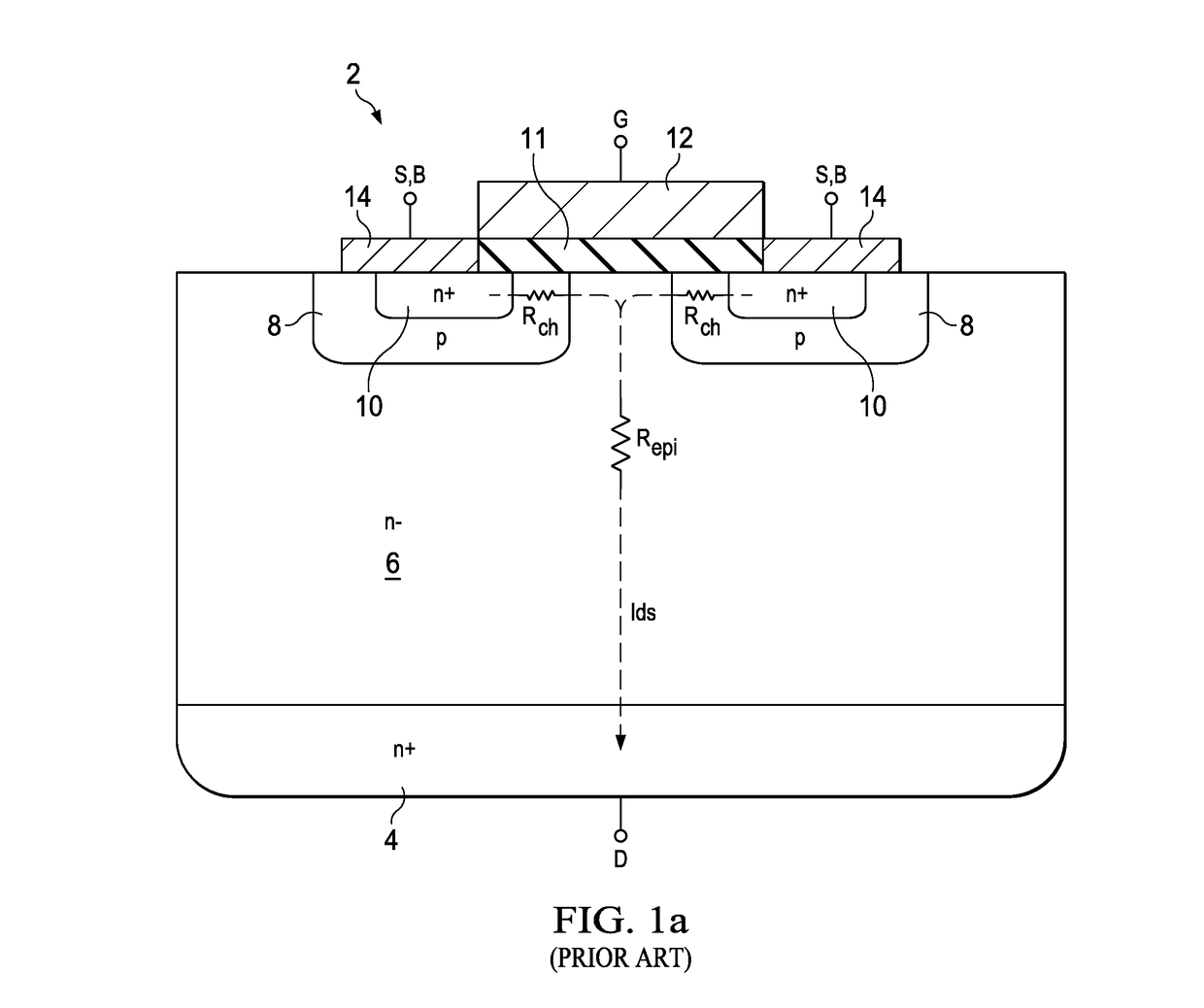
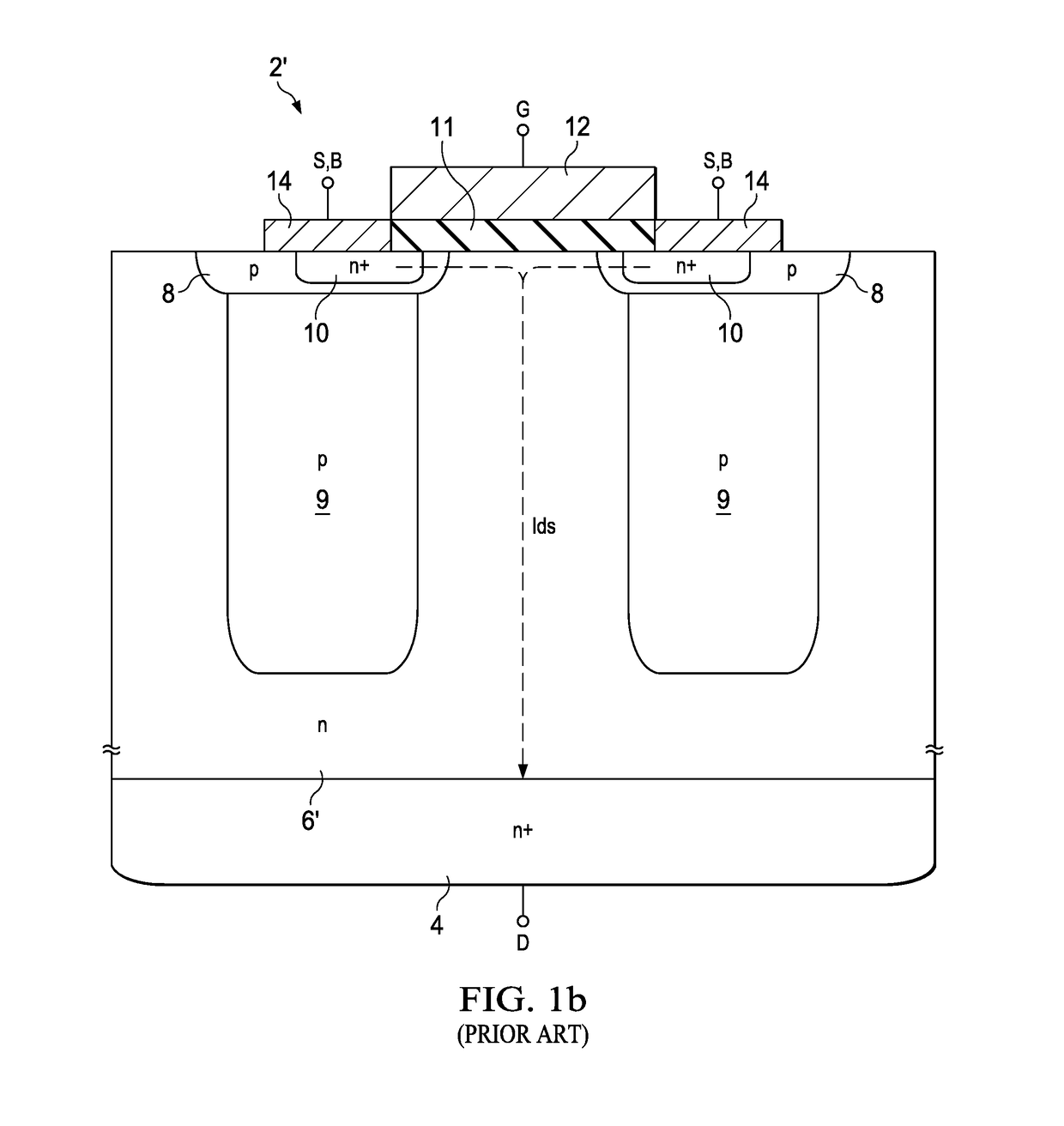
[0029]The one or more embodiments described in this specification are implemented into vertical drift metal-oxide-semiconductor (VDMOS) field-effect transistors of the superjunction type, as it is contemplated that such implementation is particularly advantageous in that context. However, it is also contemplated that concepts of this invention may be beneficially applied to other applications, for example trench gate VDMOS devices, non-superjunction VDMOS transistors, and vertical power devices of other types such as insulated gate bipolar transistors (IGBTs), vertical power diodes, and the like. Accordingly, it is to be understood that the following description is provided by way of example only, and is not intended to limit the true scope of this invention as claimed.

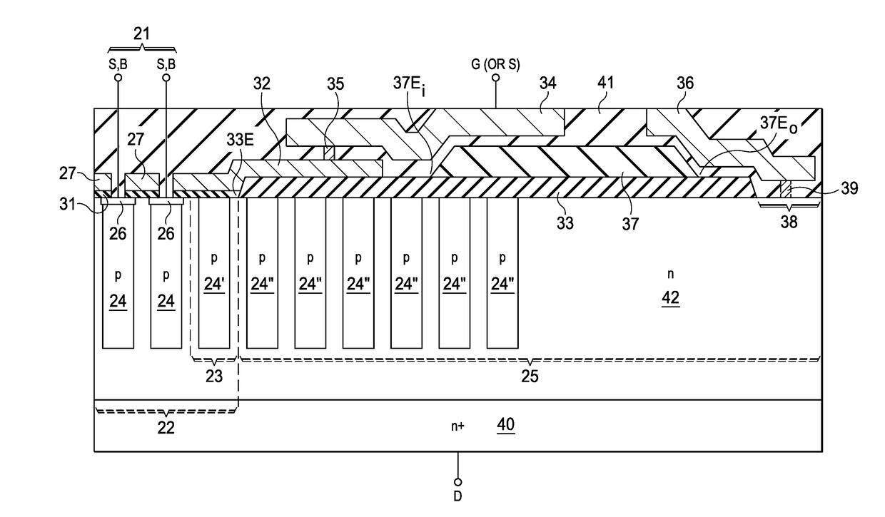
[0030]As mentioned above in the Background of the Invention, the design of the termination region of a vertical power switching device, such as a power VDMOS device, IGBT, vertical power diode, and the like, is import...


PUM


Abstract

A vertical power switching device, such as a vertical superjunction metal-oxide-semiconductor field-effect-transistor (MOSFET), in which termination structures in the corners of the integrated circuit are stretched to efficiently shape the lateral electric field. Termination structures in the device include such features as doped regions, field plates, insulator films, and high-voltage conductive regions and elements at the applied substrate voltage. Edges of these termination structures are shaped and placed according to a 2nd-order smooth, non-circular analytic function so as to extend deeper into the die corner from the core region of the device than a constant-distance path. Also disclosed are electrically floating guard rings in the termination region, to inhibit triggering of parasitic p-n-p-n structures.

Description

CROSS-REFERENCE TO RELATED APPLICATIONS[0001]Not applicable.STATEMENT REGARDING FEDERALLY SPONSORED RESEARCH OR DEVELOPMENT[0002]Not applicable.BACKGROUND OF THE INVENTION[0003]This invention is in the field of semiconductor power devices. Disclosed embodiments are directed to termination regions for vertical power transistors, including metal-oxide-semiconductor superjunction transistors.[0004]As known in the art, semiconductor power switching devices are ideally capable of blocking large forward and reverse voltages with minimal current conduction when in the “off” state while conducting large currents with minimal voltage drop when in the “on” state, with minimal switching times and minimal switching power consumption. Improvements in manufacturing yield and reduction in manufacturing cost are also sought. Advances toward these ideal attributes have largely been made in modern power transistors through innovations in device architecture, rather than through shrinking of device fe...

Claims


Application Information

Patent Timeline
Patent Type & Authority Applications(United States)
IPC IPC(8): H01L29/78H01L29/06H01L29/739H01L29/40
CPCH01L29/7811H01L29/404H01L29/7395H01L29/0619H01L29/0696H01L29/0634H01L29/8611
Inventor HARRINGTON, III, THOMAS E.SPOHNHEIMER, JOHN V.QU, ZHIJUN
Owner D3 SEMICON
Why Eureka
Try Eureka