Method for depositing dielectric film in trenches by peald

a dielectric film and trench technology, applied in the direction of chemical vapor deposition coating, coating, plasma technique, etc., can solve the problems of insufficient resolution of the etch rate of the difference between the sidewall and the top surface etch rate, so as to improve the quality of the dielectric film

Active Publication Date: 2017-04-20
ASM IP HLDG BV
View PDF6 Cites 338 Cited by
  • Summary
  • Abstract
  • Description
  • Claims
  • Application Information

AI Technical Summary

Benefits of technology

[0007]In some embodiments of the present invention, instead of improving the quality of a dielectric film at a sidewall of a trench of a substrate, by degrading the quality of a dielectric film on a top surface of the substrate, the etch rates of the film at the sidewall and on the top surface are substantially matched.
[0008]Some embodiments provide a method for substantially equalizing the quality of a film at a sidewall of a trench of a substrate and that on a top surface of the substrate by controlling process parameters such as RF power in deposition processes of a dielectric film on a substrate having trenches by PEALD using a precursor having —N(CH3)2 as a functional group. In some embodiments, the etch rate of a film on the top surface is increased by increasing RF power, whereby the quality of the film deposited on the top surface is degraded, thereby decreasing the difference in etch rate between the sidewall and the top surface. In some embodiments, the quantity of impurities (e.g., nitrogen) in the film on the top surface is increased by controlling deposition processes. The etch rate of a film is related to the quantity of impurities in the film, and by increasing the quantity of impurities, the etch rate can be increased. The quantity of impurities can be controlled by adjusting RF power, for example. By controlling deposition processes, the difference in etch rate between the sidewall and the top surface is decreased by substantially equalizing the quantity of impurities in the film at the sidewall and that on the top surface.

Problems solved by technology

In PEALD, since a sidewall of a trench of a substrate undergoes less ion bombardment than does a top surface of the substrate, surface reaction at the sidewall is less active than on the top surface, causing a problem that an etch rate of a film at the sidewall is different from (higher than) that on the top surface.
However, the improvement is partial, and the problem in different etch rates between the sidewall and the top surface is not sufficiently resolved.

Method used


Image

  • Method for depositing dielectric film in trenches by peald
  • Method for depositing dielectric film in trenches by peald
  • Method for depositing dielectric film in trenches by peald

Examples


example 1

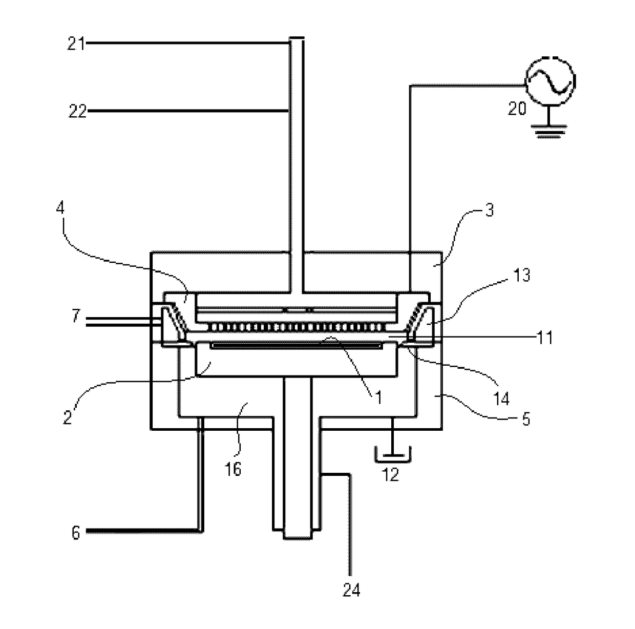
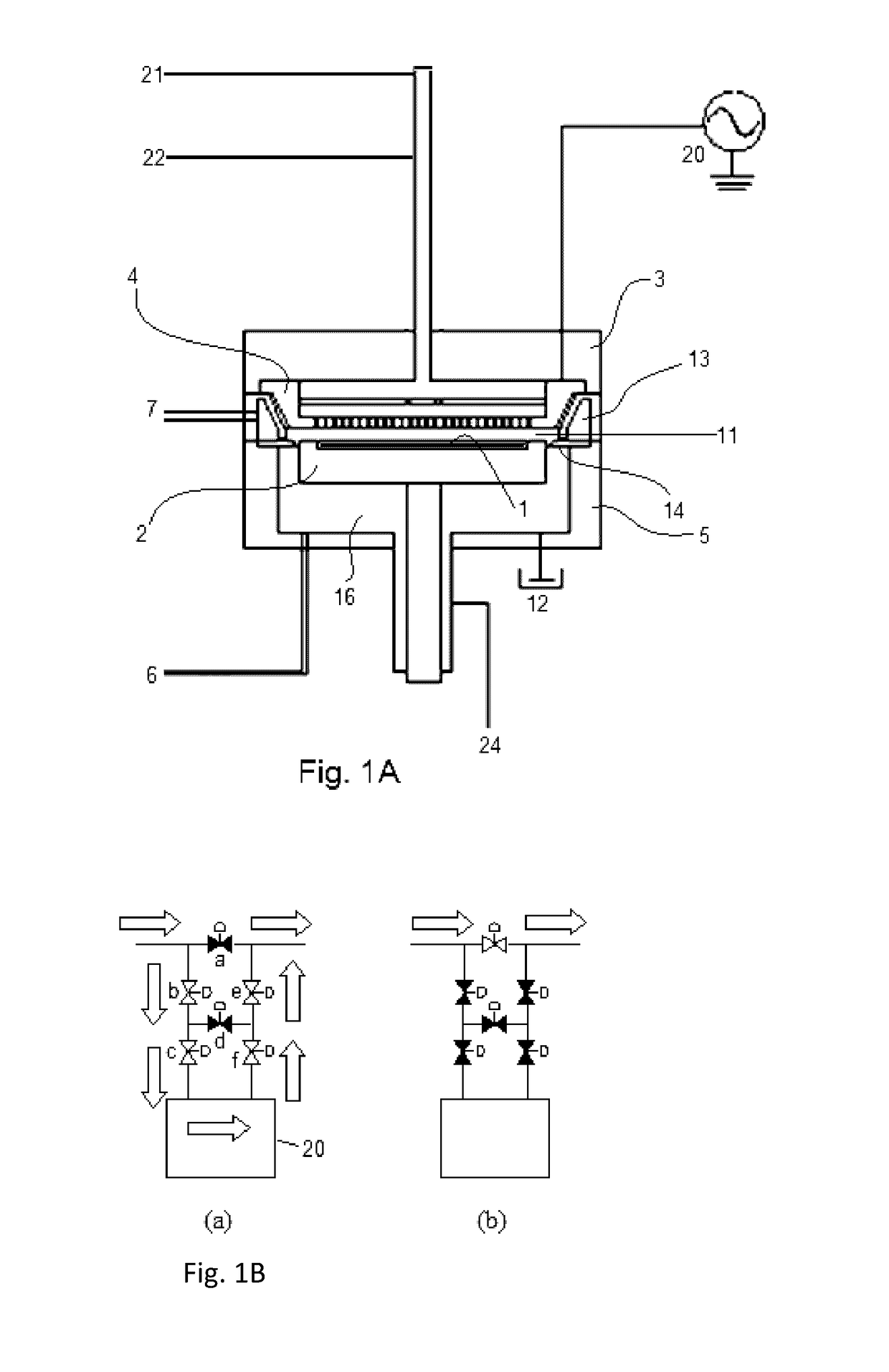
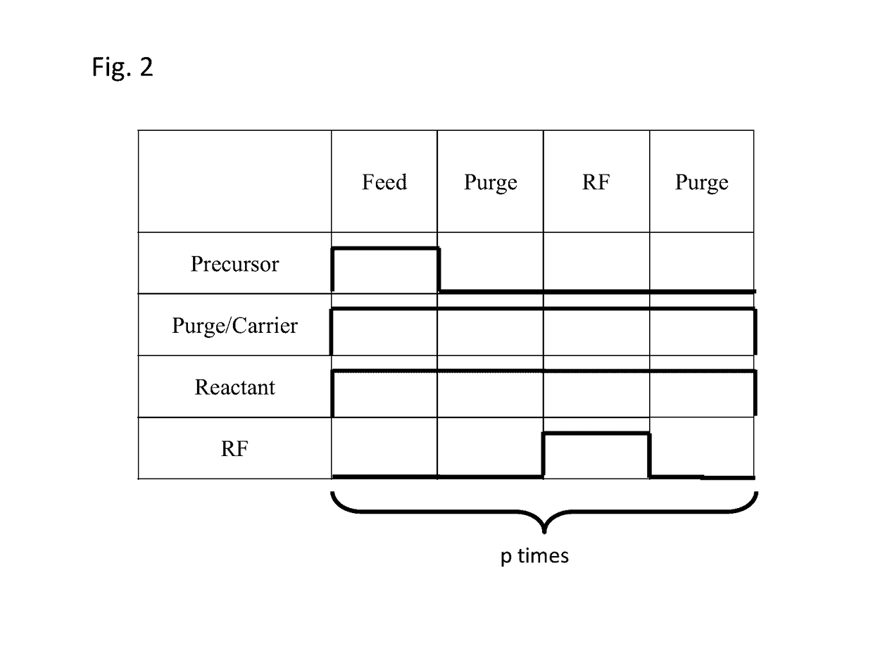
[0047]A titanium oxide film was formed on a 300-mm substrate having a patterned surface having an aspect ratio of about 2 and an opening depth of about 320 nm under the conditions shown in Table 3 below using the sequence illustrated in FIG. 2 and the PEALD apparatus illustrated in FIGS. 1A and 1B.

TABLE 3Conditions for Deposition CycleSubstrate temperature200° C.Pressure250 PaPrecursorTetrakis(dimethylamido)titaniumPrecursor pulse0.4 secPrecursor purge0.3 secReactantoxygen plasmaFlow rate of reactant (continuous)500 sccmCarrier gasargonDilution gasargonFlow rate of carrier gas (continuous)1000 sccmFlow rate of dilution gas (continuous)500 sccmRF power (13.56 MHz) for a 300-mmSee FIG. 3BwaferRF power pulse0.4 secPurge0.1 secGrowth rate per cycle0.062 to 0.065 nm / cycleTotal thickness [nm]18.6 to 19.4 nm

[0048]The wet etch rate of a part of each film deposited on the top surface of the substrate was measured. The results are shown in FIG. 3B wherein the wet etch rate is expressed as WER...

example 2

[0049]Films were deposited under the same conditions as in Example 1, and the wet etch rate of each film not only on the top surface but also at the sidewall was measured. The results are shown in FIG. 4. As shown in FIG. 3B, the wet etch rate began increasing after hitting the minimum value (the lowest vertex), and FIG. 4 shows the wet etch rate after the lowest vertex. The quality of the film on the top surface obtained at the lowest vertex appears to be the highest. Although the quality of the film on the top surface was the highest at the lowest vertex, the quality of the film at the sidewall was not high, i.e., the wet etch rate of the film at the sidewall was relatively high. Since plasma does not easily reach the sidewall, the quality of the film at the sidewall is not significantly affected by the intensity of RF power, in contrast with the quality of the film on the top surface. The wet etch rate of the film at the sidewall gradually decreased as RF power increased as shown...

example 3

[0050]The film deposited in a trench when RF power was 200 W was analyzed by Scanning transmission electron microscopy (STEM). FIG. 5 shows STEM photographs of cross-sectional views of the film, wherein (a) shows the film as deposited, and (b) shows the film after wet etching. As shown in FIG. 5, the conformality of the film as deposited was 89% at the upper sidewall, 96% at the lower sidewall, and 97% at the bottom, whereas the conformality of the film after wet etching was 83% at the upper sidewall, 90% at the lower sidewall, and 89% at the bottom, i.e., the conformality of the film decreased after wet etching by about 6% to about 8%.

[0051]Also, the film deposited in a trench when RF power was 500 W was analyzed by Scanning transmission electron microscopy (STEM). FIG. 6 shows STEM photographs of cross-sectional views of the film, wherein (a) shows the film as deposited, and (b) shows the film after wet etching. As shown in FIG. 6, the conformality of the film as deposited was 83%...


PUM

PropertyMeasurementUnit
depthaaaaaaaaaa
aspect ratioaaaaaaaaaa
thicknessaaaaaaaaaa

Abstract

A method for depositing a dielectric film in a trench by plasma-enhanced atomic layer deposition (PEALD) includes depositing a dielectric film in a trench of a substrate by PEALD under conditions wherein the wet etch rate of the depositing film on a top surface of the substrate is substantially equivalent to or higher than the wet etch rate of the depositing film at a sidewall of the trench, wherein a precursor fed into the reaction space has —N(CH3)2 as a functional group.

Description

BACKGROUND OF THE INVENTION[0001]Field of the Invention[0002]The present invention generally relates to a method for depositing a dielectric film in a trench of a substrate by plasma-enhanced atomic layer deposition (PEALD).[0003]Description of the Related Art[0004]In PEALD, since a sidewall of a trench of a substrate undergoes less ion bombardment than does a top surface of the substrate, surface reaction at the sidewall is less active than on the top surface, causing a problem that an etch rate of a film at the sidewall is different from (higher than) that on the top surface.[0005]Conventionally, by increasing the process temperature or the like, the quality of a dielectric film (e.g., density, hardness) deposited on a sidewall is improved so that the etch rate at the sidewall can be decreased. However, the improvement is partial, and the problem in different etch rates between the sidewall and the top surface is not sufficiently resolved.[0006]Any discussion of problems and solut...

Claims


Application Information

Patent Timeline
Patent Type & Authority Applications(United States)
IPC IPC(8): C23C16/50C23C16/52H01J37/32
CPCC23C16/50H01J37/32009H01J2237/3321H01J2237/334C23C16/52C23C16/44H01L21/02271C23C16/045C23C16/405C23C16/45542C23C16/45561H01J37/32082H01L21/02274H01L21/0228H01L21/02315H01L21/28194H01L21/30604H01L21/76831H05H1/46
Inventor SUEMORI, HIDEMI
Owner ASM IP HLDG BV
Why Eureka
Try Eureka