NbMC LAYERS

a technology of nbmc layers and gate channels, applied in the direction of coatings, semiconductor devices, chemical vapor deposition coatings, etc., can solve the problems of loss of desired device performance, difficult modification of threshold voltage of devices, and difficult tuning of work function differences between gate and channel, etc., to achieve low work function, low resistance, and easy tuning

Active Publication Date: 2017-04-27
ASM IP HLDG BV
View PDF3 Cites 312 Cited by
  • Summary
  • Abstract
  • Description
  • Claims
  • Application Information

AI Technical Summary

Problems solved by technology

However, by replacing polysilicon with metal, a work function difference between the gate and the channel becomes more difficult to tune.
As a result, modification of a threshold voltage of the device becomes more difficult.
Generally, the work-function layers are relatively less conductive than gate electrode metal, which can result in a loss of desired performance of the devices.
Attempts to increase the conductivity of the work-function layers generally results in lower work function of the devices.

Method used


Image

  • NbMC LAYERS
  • NbMC LAYERS
  • NbMC LAYERS

Examples


Embodiment Construction

[0021]The description of exemplary embodiments of methods, structures, and devices provided below is merely exemplary and is intended for purposes of illustration only; the following description is not intended to limit the scope of the disclosure or the claims. Moreover, recitation of multiple embodiments having stated features is not intended to exclude other embodiments having additional features or other embodiments incorporating different combinations of the stated features.

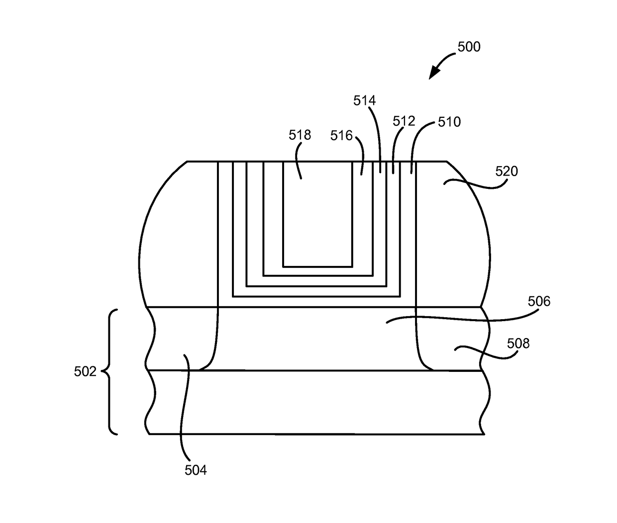
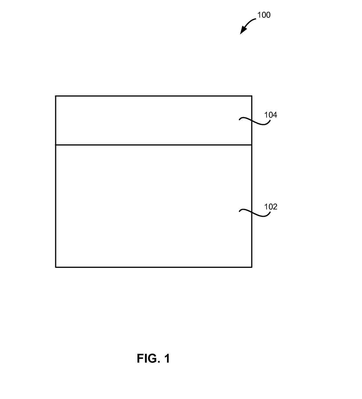
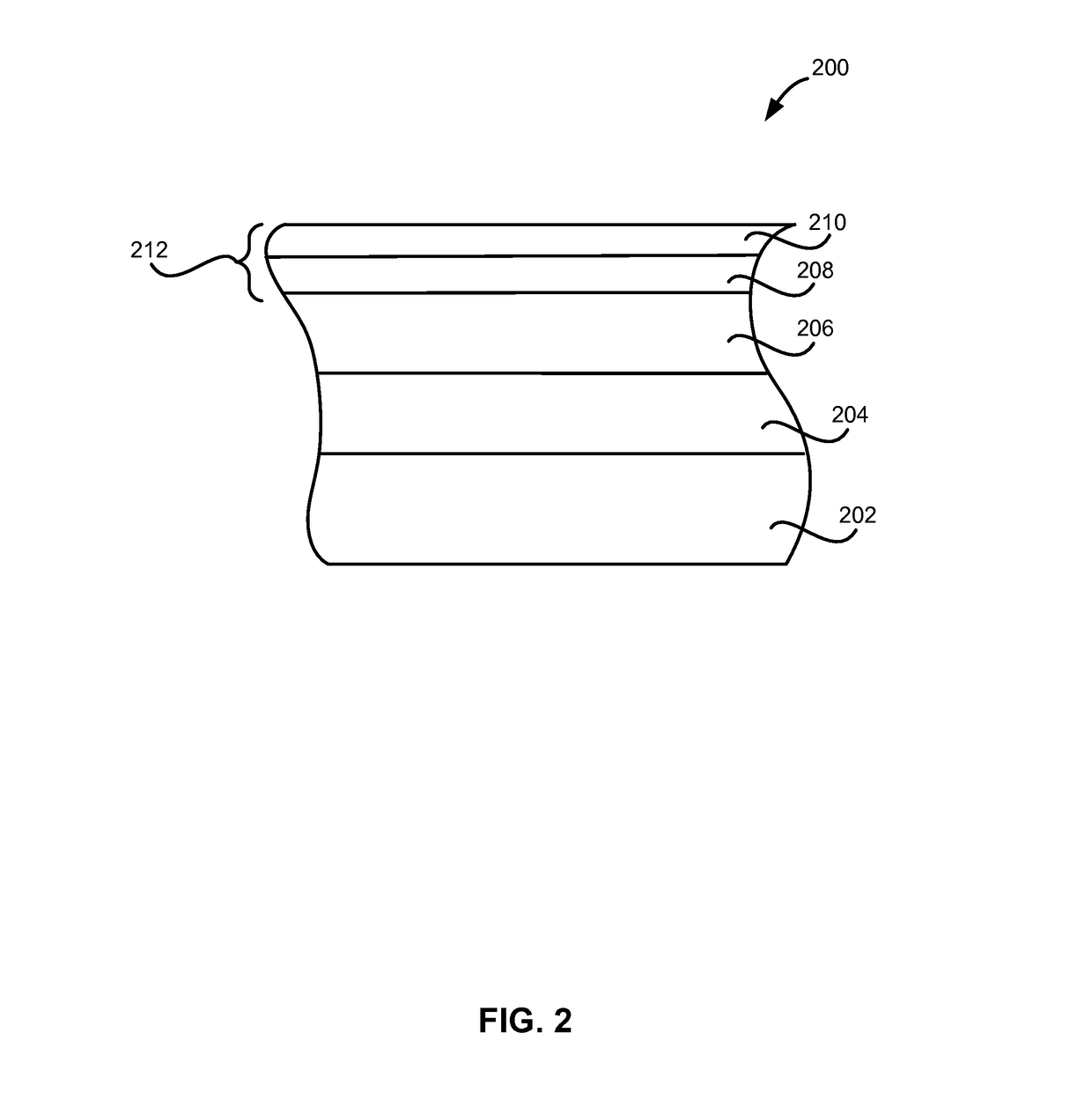
[0022]Exemplary embodiments of the present disclosure relate to methods of depositing NbMC layers onto a substrate and to structures and devices including one or more NbMC layers. Exemplary NbMC layers include niobium, a metal and / or metalloid, and carbon. The metal can include one or more metals, such as a Group 13 metal (e.g., aluminum); the metalloid can include one or more metalloids (e.g. boron). The niobium NbMC films can also include other elements, such as nitrogen, hydrogen, trace amounts of other m...


PUM

PropertyMeasurementUnit
work functionaaaaaaaaaa
thicknessaaaaaaaaaa

Abstract

Methods of forming thin-film structures including one or more NbMC layers, and structures and devices including the one or more NbMC layers are disclosed. The NbMC layers enable tuning of various structure and device properties, including resistivity, current leakage, and work function.

Description

FIELD OF THE INVENTION[0001]The present disclosure generally relates to techniques for forming structures including one or more niobium metal or metalloid carbide (NbMC) layers, to devices including the one or more niobium metal or metalloid carbide layers, and to methods of forming the structures and devices.BACKGROUND OF THE DISCLOSURE[0002]Field-effect transistor (FET) devices, such as metal-oxide-semiconductor FET (MOSFET) devices generally include a source region, a drain region, a channel region between the source and drain regions, and a gate electrode overlying the channel region and separated from the channel region by a dielectric material. A complimentary MOSFET (CMOS) device includes a p-type MOSFET device and an n-type MOSFET device. There are also three-dimensional transistor architectures like FinFET's. To operate as desired, a work function of the gate electrode of the n-type device and of the p-type device must differ by a certain amount. The difference in the work ...

Claims


Application Information

Patent Timeline
Patent Type & Authority Applications(United States)
IPC IPC(8): H01L21/02H01L29/51
CPCH01L21/02194H01L29/517H01L21/02205H01L21/0228H01L21/28562H01L21/32051C23C16/045C23C16/32C23C16/45531C23C16/45536H01L21/28088H01L29/78H01L29/4966
Inventor ZHU, CHIYUASIKAINEN, TIMOMILLIGAN, ROBERT BRENNAN
Owner ASM IP HLDG BV
Why Eureka
Try Eureka