LED lighting unit

a technology of led lighting and lighting components, which is applied in the field of led lighting units, can solve the problems of high temperature exposure of optical components, difficult to tolerate, and limit the amount of light that can be generated, and achieve the effects of low cost and high thermal and optical stability

Active Publication Date: 2017-05-04
KONINKLJIJKE PHILIPS NV
View PDF18 Cites 15 Cited by
  • Summary
  • Abstract
  • Description
  • Claims
  • Application Information

AI Technical Summary

Benefits of technology

[0019]This design is preferably able to withstand the short duration high temperatures encountered during reflow soldering, so that even with a small unit height, it can be soldered to an underlying printed circuit board, for example. During this reflow soldering, the microstructured layer should remain dimensionally stable (no size loss) with no wrinkling or bulging, and additionally no yellowing. This may not be possible for some conventional materials such as an acrylic resin-on polycarbonate base layer.
[0041]In some of these examples, the phosphor layer may thus be larger in area than the light output area of the LED, thereby providing a more uniform illumination to the optical layer or layers above.

Problems solved by technology

In addition to physical dimension limitations, there are specific requirements to the beam profile that is emitted by a flash LED package.
This means a smaller LED, which gives limitations to the amount of light that can be generated.
A problem with such small build heights is that the optical component (either Fresnel lens or other collimating optics) is very close to the location where the unit is mounted on an underlying circuit board.
If reflow soldering is used to mount the LED unit on a circuit board, the optical components are exposed to high temperatures, which may not be easily tolerated by the optical component design.

Method used


Image

  • LED lighting unit
  • LED lighting unit
  • LED lighting unit

Examples


Embodiment Construction

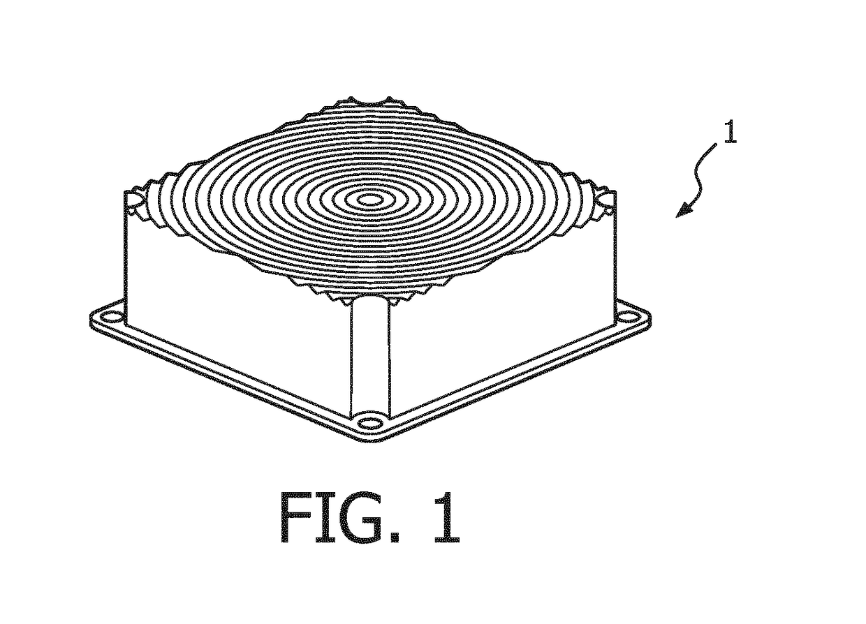
[0061]The invention provides an LED-based lighting unit which comprises a support structure, an LED-based light emitting structure and an optical beam shaping arrangement over the top of the support structure. The optical beam shaping arrangement comprises a thermally stable microstructured layer, and the (underside of the) beam shaping arrangement is at a small height above the LED-based light emitting structure. The height is less than the square root of a light emitting area of the LED-based light emitting structure (10). For example, for a light emitting area of 1 mm2, the height is less than 1 mm, for example less than 0.5 mm.

[0062]The optical beam shaping arrangement is designed to enable the lighting unit to be mounted on a carrier by reflow soldering without damaging the optics.

[0063]The optical beam shaping arrangement used in the system of the invention performs a beam shaping function. This function may for example approximate at least a partial collimation function, in t...


PUM


Abstract

An LED lighting unit comprising a support structure (14), an LED-based light emitting structure (10) mounted within the support structure and an optical beam shaping arrangement (50, 52) over the top of the support structure. The optical beam shaping arrangement comprises an optically transparent and thermally stable material, and the support structure supports the microstructured layer at a small height above the LED-based light emitting structure. This height may for example be less than 0.5 mm. The optical beam shaping arrangement enables a compact and low height lighting unit to be mounted on a carrier by reflow soldering without damaging the optical beam-shaping component.

Description

FIELD OF THE INVENTION[0001]This invention relates to LED lighting units, for example for use in camera or video flash applications, such as flash units for mobile phones or other portable mobile device such as tablets and laptop computers.BACKGROUND OF THE INVENTION[0002]There is a trend to miniaturize LED lighting units. A compact LED lighting unit can for example be considered to be a lighting unit with a package height less than 3 mm, and an output aperture with an area of less than 100 mm2. A compact lighting unit of this type can be integrated into a portable device such as a mobile phone.[0003]Compact LED lighting units such as flash LED packages typically consist of high power LEDs to generate white light, usually at a colour temperature of about 5000-6500 K, combined with Fresnel optical lenses either through integration with the LED package directly or with a separate housing for the lens and the LED package.[0004]These packages typically use a high power blue LED covered ...

Claims


Application Information

Patent Timeline
Patent Type & Authority Applications(United States)
IPC IPC(8): H04N5/225F21K9/64H01L33/50F21V5/00F21V17/10F21V33/00G02B19/00
CPCH04N5/2256F21V33/0052H04N5/2253F21K9/64F21Y2115/10F21V5/002F21V17/101H01L33/502H01L33/505G02B19/0061G03B15/05G03B2215/0567G03B2215/0592H05B33/14H04N23/54H04N23/56
Inventor JAGT, HENDRIK JOHANNES BOUDEWIJNCROMPVOETS, FLORIS MARIA HERMANSZDEKKERS, WOUTERZAHN, FRITZ HELMUTVDOVIN, OLEXANDR VALENTYNOVYCHHEUTS, JACOBUS JOHANNES FRANCISCUS GERARDUSSANDER-JOCHEM, MARIA JOHANNA HELENAKLEIJNEN, CHRISTIAN
Owner KONINKLJIJKE PHILIPS NV
Why Eureka
Try Eureka