Computer addressable plasma density modification for etch and deposition processes

a plasma density and etching technology, applied in the field of computer addressable plasma density modification for etching and deposition processes, can solve the problems of differential across-wafer activation of plasma-mediated surface reactions, inability to maintain ideal plasma density, and inability to achieve the ideal degree of uniformity

Inactive Publication Date: 2017-05-11
LAM RES CORP
View PDF21 Cites 128 Cited by
  • Summary
  • Abstract
  • Description
  • Claims
  • Application Information

AI Technical Summary

Problems solved by technology

However, these processes do not always proceed with the ideal degree of uniformity across the entire surface of the substrate being processed.
For the case of plasma-based processes (and due to the highly energized nature of the plasma phase), it may be that it is difficult to maintain an ideally uniform plasma density in the spatial region where it contacts the substrate surface, and these differences in plasma density may lead to differential across-wafer activation of plasma-mediated surface reactions (whether deposition or etching).
However, many other factors besides plasma characteristics may also contribute, in whole or in part, to wafer non-uniformity.
Other systematic non-uniformities may include wafer center-to-edge non-uniformities occurring because of the intrinsic wafer size / geometry.
Of course, substrate processing non-uniformities may also be random, e.g., the result of random fluctuations in reaction chamber process conditions, random wafer variation, etc.
More typically, both systematic and random factors contribute to non-uniformities in substrate processing.

Method used


Image

  • Computer addressable plasma density modification for etch and deposition processes
  • Computer addressable plasma density modification for etch and deposition processes
  • Computer addressable plasma density modification for etch and deposition processes

Examples


Embodiment Construction

[0022]In the following description, numerous specific details are set forth in order to provide a thorough understanding of the present invention. However, the present invention may be practiced without some or all of these specific details. In other instances, well known process operations have not been described in detail so as to not unnecessarily obscure the present invention. While the invention will be described in conjunction with specific detailed embodiments, it is to be understood that these specific detailed embodiments are not intended to limit the scope of the inventive concepts disclosed herein.

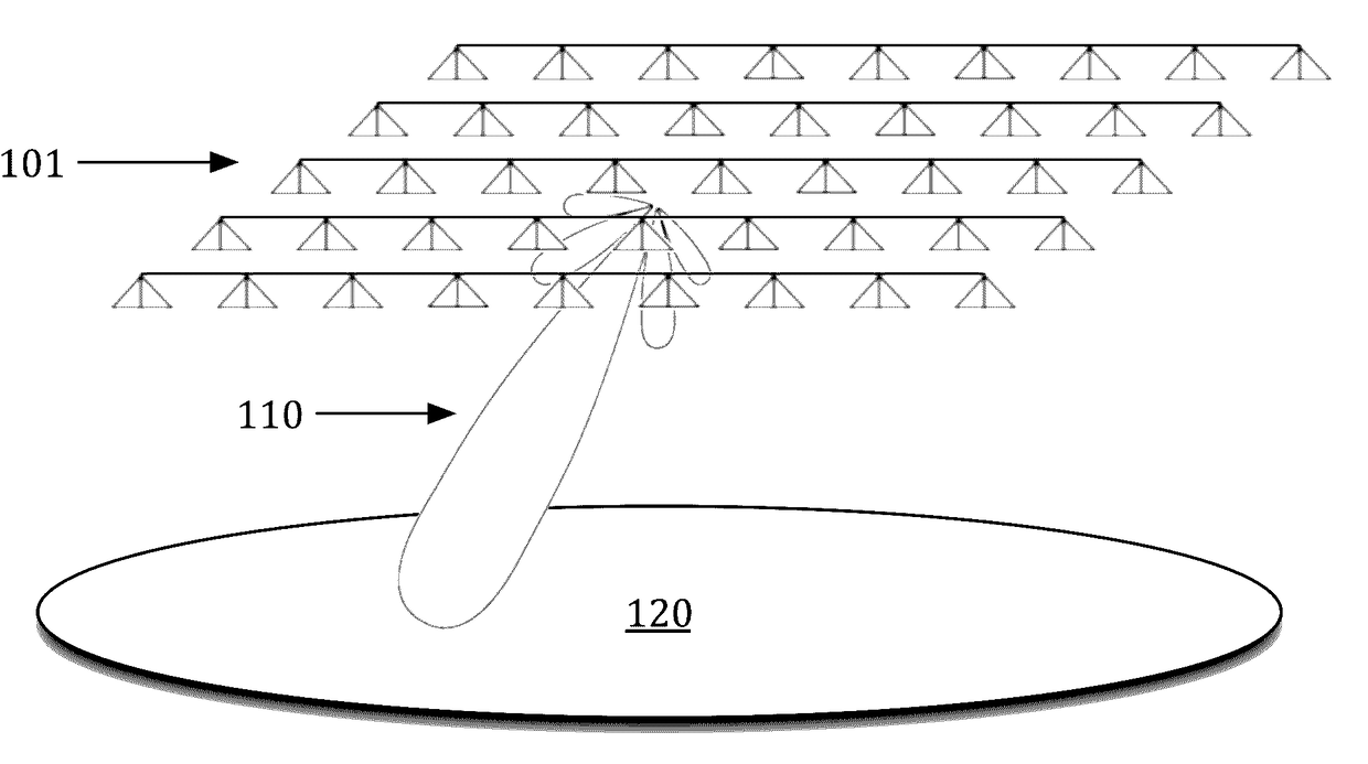
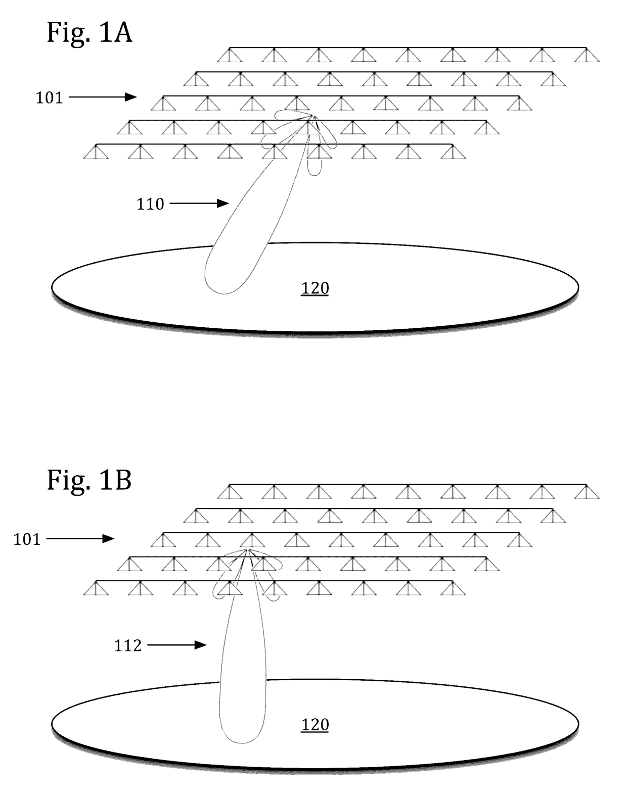
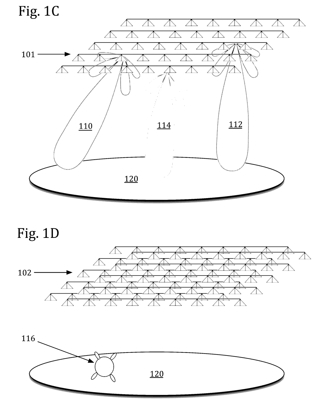
[0023]Although it is generally desired that wafer processing operations apply with uniform effect consistently across the entire surface of every wafer that is processed, such uniformity, of course, is not a reality. In reality, wafer processing operations exhibit across-wafer non-uniformity to varying degrees. In some cases, non-uniformities in a deposited and / or etched film ma...


PUM

PropertyMeasurementUnit
diameteraaaaaaaaaa
diameteraaaaaaaaaa
diameteraaaaaaaaaa

Abstract

Disclosed herein are methods of modifying a reaction rate on a semiconductor substrate in a processing chamber which utilize a phased-array of microwave antennas. The methods may include energizing a plasma in a processing chamber, emitting a beam of microwave radiation from a phased-array of microwave antennas, and directing the beam into the plasma so as to cause a change in a reaction rate on the surface of a semiconductor substrate inside the processing chamber. Also disclosed herein are particular embodiments of phased-arrays of microwave antennas, as well as semiconductor processing apparatuses which include a phased-array of microwave antennas configured to emit a beam of microwave radiation into a processing chamber.

Description

BACKGROUND[0001]Many classes of processes important in semiconductor fabrication involve the use of a gas plasma. Reactive ion etching (RIE) operations and atomic layer deposition (ALD) operations, for example, may involve the use of energetic plasma-phase ion and free-radical species to activate their associated surface reactions—surface etch reactions for the case of RIE and surface deposition reactions for the case of ALD. However, these processes do not always proceed with the ideal degree of uniformity across the entire surface of the substrate being processed. Many factors can affect across-wafer uniformity. For the case of plasma-based processes (and due to the highly energized nature of the plasma phase), it may be that it is difficult to maintain an ideally uniform plasma density in the spatial region where it contacts the substrate surface, and these differences in plasma density may lead to differential across-wafer activation of plasma-mediated surface reactions (whether...

Claims


Application Information

Patent Timeline
Patent Type & Authority Applications(United States)
IPC IPC(8): H01J37/32C23C16/455H01L21/3065C23C16/511H01L21/67H01L21/02
CPCH01J37/3222H01L21/67069H01L21/0228H01L21/3065H01J37/32926H01J2237/3321C23C16/511C23C16/45544C23C16/45565H01J37/3244H01J2237/3341H01J37/32238H01J37/32091H01J37/3211H01Q21/00H01Q21/061H01J37/321H01J37/32449H01J37/32899H01L21/02315H01L21/32136H05H1/46
Inventor BERRY, III, IVAN L.
Owner LAM RES CORP
Why Eureka
Try Eureka