

Showerhead-cooler system of a semiconductor-processing chamber for semiconductor wafers of large area
a technology of semiconductor wafers and coolers, which is applied in the field of semiconductor production, can solve problems such as non-uniform etching
- Summary
- Abstract
- Description
- Claims
- Application Information
AI Technical Summary
Benefits of technology
Problems solved by technology
Method used
Image

Examples
Embodiment Construction
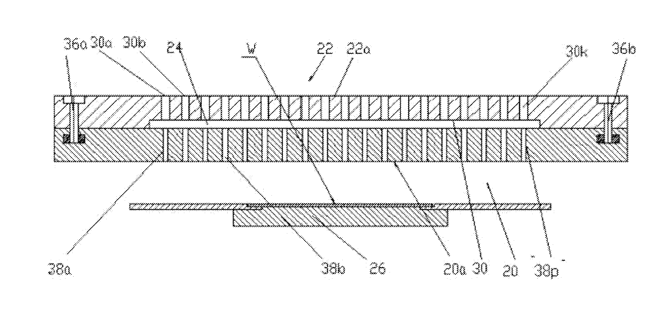
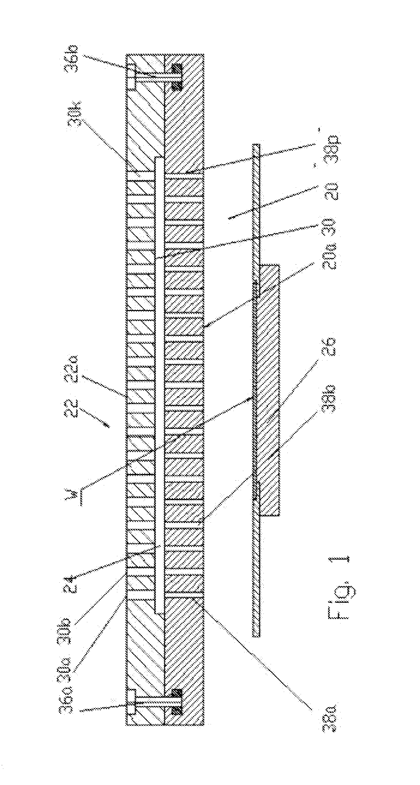
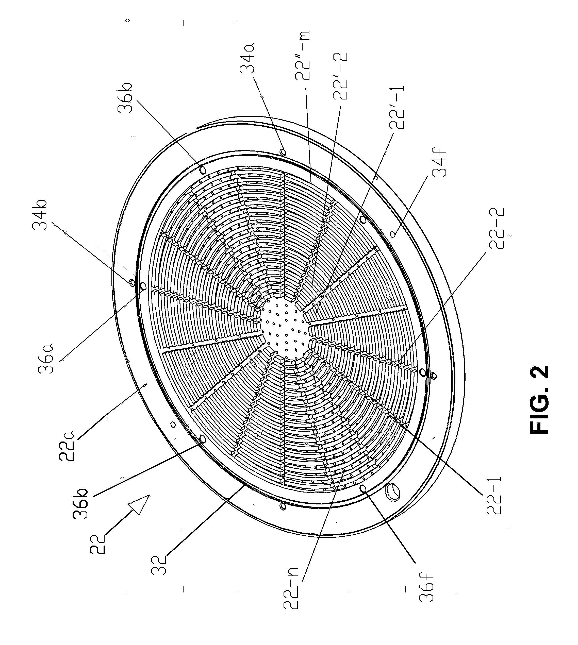
[0097]The present invention relates to a deterioration-resistant showerhead-cooler system of a semiconductor-processing chamber with uniform distribution of plasma density that includes a system of a showerhead with a gas-feeding cooler plate (hereinafter referred to as “system”) for use in a semiconductor-processing chamber that provides uniform distribution of plasma density in the working cavity of the chamber over the surface of a semiconductor wafer having an increased diameter, e.g., up to 450 mm. It has been found that etching of large-diameter wafers, e.g., 450 mm in diameter, in a CCP plasma-treatment apparatus requires that for generating plasma of sufficiently high density, a power source of very high frequency up to 150 MHz be used. However, such high frequencies adversely affect distribution of plasma density and lead to nonuniformity of etching. In plasma-treatment apparatuses of the aforementioned type, plasma density depends on the radius of the showerhead, which is ...
PUM
| Property | Measurement | Unit |
|---|---|---|
| Angle | aaaaa | aaaaa |
| Angle | aaaaa | aaaaa |
| Diameter | aaaaa | aaaaa |
Abstract
Description
Claims
Application Information