Method of initializing 3D non-volatile memory device

a non-volatile memory and nand flash memory technology, applied in static storage, digital storage, instruments, etc., can solve the problems of increasing the downscaling difficulty of the conventional two-dimensional (2d) the difficulty of downscaling the conventional 2d memory cell array architecture, so as to increase the integration degree of the 3d non-volatile memory device

Active Publication Date: 2017-05-18
SK HYNIX INC +1
View PDF5 Cites 40 Cited by
  • Summary
  • Abstract
  • Description
  • Claims
  • Application Information

AI Technical Summary

Benefits of technology

[0010]Embodiments of the present disclosure provide a method of initializing a 3D non-volatile memory device for multi-level programming string selection transistors, such that the string selection transistors have thre

Problems solved by technology

Recently, downscaling the NAND flash memory device with a conventional two-dimensional (2D) memory cell array architecture has become more difficult as 20 nm or smaller photolithography techniques have reached their limits.
In addition, design issues, which are related to reductio

Method used


Image

  • Method of initializing 3D non-volatile memory device
  • Method of initializing 3D non-volatile memory device
  • Method of initializing 3D non-volatile memory device

Examples


Embodiment Construction

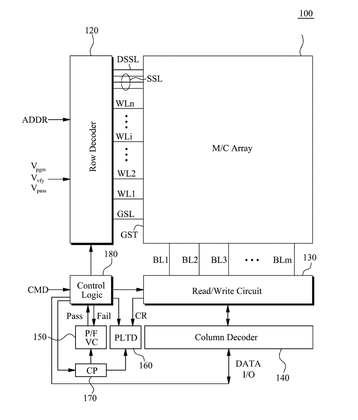
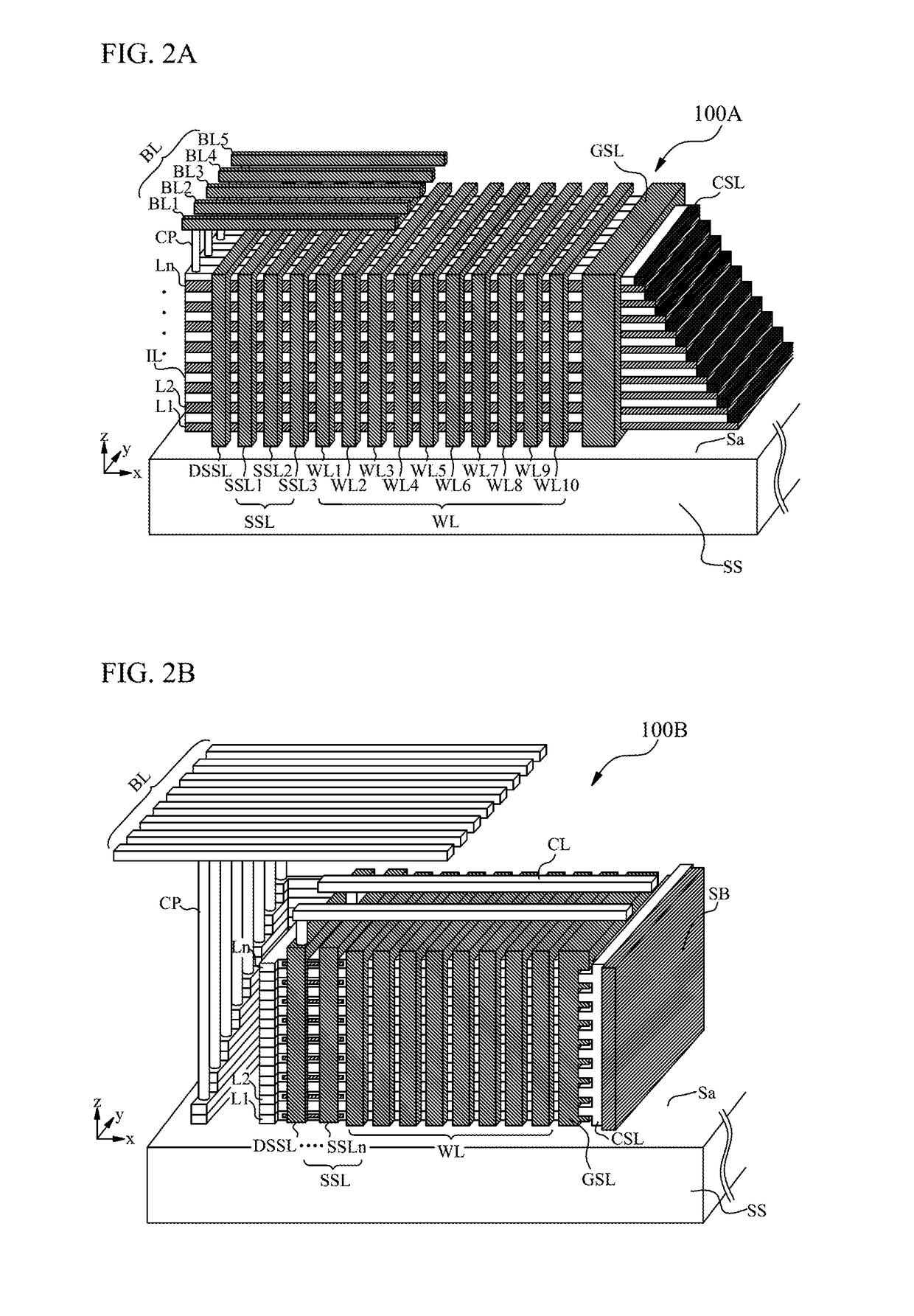
[0038]The present disclosure will now be described more fully with reference to the accompanying drawings, in which exemplary embodiments of the invention are shown. The invention may, however, be embodied in many different forms and should not be construed as being limited to the embodiments set forth herein; rather, these embodiments are provided so that this disclosure will be thorough and complete, and will fully convey the concept of the invention to those skilled in the art.

[0039]Like numbers refer to like elements throughout. As used herein, the term “and / or” includes any and all combinations of one or more of the associated listed items.

[0040]The terminology used herein is for the purpose of describing particular embodiments only and is not intended to be limiting of the invention. As used herein, the singular forms “a”, “an” and “the” are intended to include the plural forms as well, unless the context clearly indicates otherwise. It will be further understood that the term...


PUM


Abstract

A 3D non-volatile memory device may include a dummy string selection line, string selection lines, wordlines, bitlines, a ground selection line, and memory layers. Each of the memory layers comprising channel lines respectively coupled to the bitlines via first ends and coupled to a common source line of the memory layer via second ends. The dummy string selection line, the string selection lines, the wordlines, and the ground selection line intersect with the channel lines, and each of the channel lines defines a memory string. Initializing the 3D non-volatile memory device may include programming string selection transistors coupled with the string selection lines to have one or more threshold values, and programming a dummy string selection transistor coupled with the dummy string selection line to have a predetermined threshold value, such that the dummy string selection transistor together with the string selection transistors function as string selection transistors.

Description

CROSS-REFERENCES TO RELATED APPLICATION[0001]The present application claims the benefit of Korean application number 10-2015-0160049, filed on Nov. 14, 2015, which is herein incorporated by reference in its entirety.BACKGROUND OF THE INVENTION[0002]1. Field[0003]Embodiments of the present disclosure relate to a semiconductor memory technique, and more particularly, to a method of initializing a 3D non-volatile memory device.[0004]2. Description of the Related Art[0005]Due to increasing demands for portable application devices, such as digital cameras, smart phones, and tablet PCs, and replacement of conventional hard disk drives with solid-state drives (SSDs), markets for non-volatile memory devices are rapidly growing. Among these non-volatile memory devices, NAND flash memory devices are popular due to low manufacturing cost for high degree of integration.[0006]Recently, downscaling the NAND flash memory device with a conventional two-dimensional (2D) memory cell array architectur...

Claims


Application Information

Patent Timeline
IPC IPC(8): G11C16/20G11C16/12G11C16/34G11C16/04G11C16/14
CPCG11C16/20G11C16/0483G11C16/12G11C16/3459G11C16/14G11C7/02G11C16/10
Inventor PARK, BYUNG GOOKKWON, DAE WOONGKIM, DO BINLEE, SANG HO
Owner SK HYNIX INC
Why Eureka
Try Eureka