Touch and pressure sensitive panel

Inactive Publication Date: 2017-06-08
LUMINOUS OPTICAL TECH
5 Cites 11 Cited by

AI-Extracted Technical Summary

Problems solved by technology

In some cases, such an operating mode may meet a difficulty, for example, a virtual key shown on a touchscreen may be unexpectedly activated because it merely needs a very light force or even does not need a force to apply thereon.
It is a serious chal...

Method used

[0025]The insulative layer 30 is a flexible transparent sheet, for example, an optical glass plate or PMMA (polymethylmethacrylate) or COP (cyclo olefin polymers) thin plate with a thickness of about 0.1 mm. Alternately, the insulative layer 30 may select a dielectric material to improve a gain of touch signal.
[0031]As shown in FIG. 2, when a touching matter 80 such as a finger nears the surface layer 10, the driving electrodes 41 near the touching matter 80 capacitively couple the touching matter 80, and then charges will be grounded from the stimulated driving electrodes 41 through the touching matter 80. This can reduce capacitance between the driving electrodes 41 and the sensing electrodes 21. This change of capacitance can be interpreted as a touching position.
[0034]In order to increase sensible capacitance between the second and third electrode layers 40, 60, the driving electrodes 41 and the sensing electrodes 61 can be formed into a grid shape with an interlacing arrangement as shown in FIG. 4. This can enhance accuracy of detection of pressure from the touching matter 80. As a result, the touch pressure sensing structure 200 can obtain var...

Benefits of technology

[0006]An object of the invention is to provide a touch and pressure sensitive panel, wh...

Abstract

The panel is composed of a touch sensing structure and a touch pressure sensing structure, which separately include functional layers. The touch sensing structure can determine the location of a touch by a change in capacitance on the surface when touching the panel. The touch pressure sensing structure has a strain isolation layer with a property of elastic deformation between electrodes for detecting pressure applied onto the panel by a change in capacitance resulting from relative displacement between two electrodes.

Application Domain

Input/output processes for data processing

Technology Topic

Pressure sensitiveRelative displacement +8

Image

  • Touch and pressure sensitive panel
  • Touch and pressure sensitive panel
  • Touch and pressure sensitive panel

Examples

  • Experimental program(1)

Example

[0017]FIG. 1 is an exploded view of the invention;
[0018]FIG. 2 is a cross-sectional view of the invention;
[0019]FIG. 3 is another cross-sectional view of the invention when being pressed;
[0020]FIG. 4 is a schematic view of patterns of the second and third electrode layers; and
[0021]FIG. 5 is a cross-sectional view of another embodiment of the invention.
DETAILED DESCRIPTION OF THE INVENTION
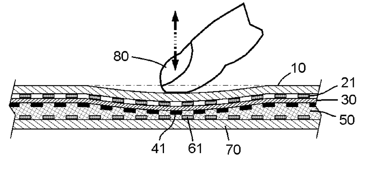
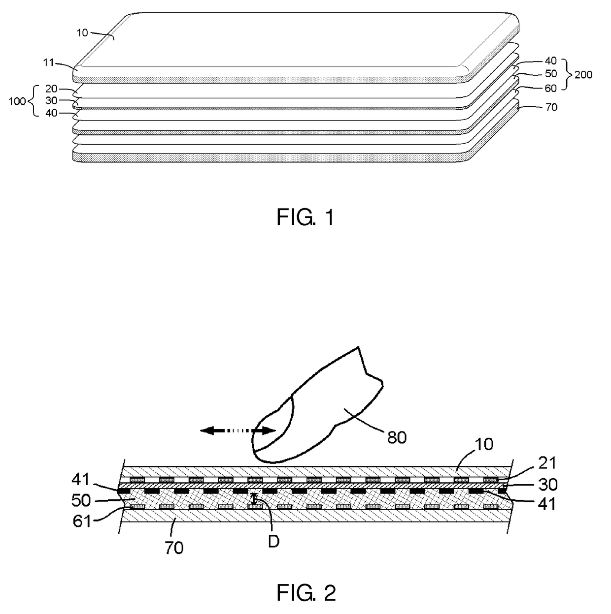
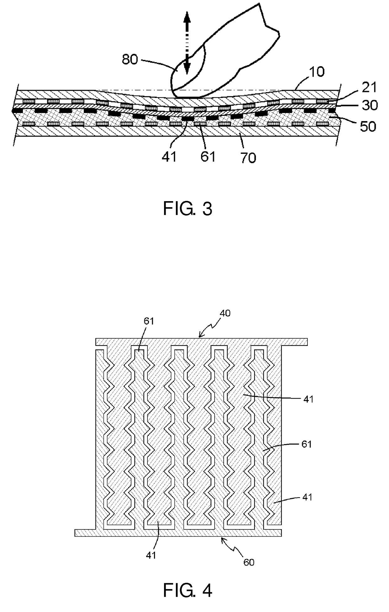
[0022]Please refer to FIGS. 1 and 2. As shown, the touch and pressure sensitive panel of the invention includes a surface layer 10, a first electrode layer 20, an insulative layer 30, a second electrode layer 40, a strain isolation layer 50, a third electrode layer 60 and a base layer 70.
[0023]The surface layer 10 is made of a transparent sheet material, such as an optical glass sheet. To make the surface layer 10 flexible, its thickness is about 0.4 mm. Also, the surface layer 10 may be further reinforced by a chemical or tempering process. Additionally, each of four corners of the surface layer 10 is formed with a chamfering 11 to prevent the surface layer 10 from peeling off.
[0024]The first electrode layer 20 is a flexible transparent conductive film, such as an ITO (indium tin oxide) conductive film, and is sandwiched between the surface layer 10 and the insulative layer 30. There are sensing electrodes 21 at regular intervals on the first electrode layer 20.
[0025]The insulative layer 30 is a flexible transparent sheet, for example, an optical glass plate or PMMA (polymethylmethacrylate) or COP (cyclo olefin polymers) thin plate with a thickness of about 0.1 mm. Alternately, the insulative layer 30 may select a dielectric material to improve a gain of touch signal.
[0026]The second electrode layer 40 is a flexible transparent conductive film, such as an ITO conductive film, and is disposed under the insulative layer 30. There are driving electrodes 41 at regular intervals on the second electrode layer 40. Preferably, an ITO conductive layer may be directly formed on each side of the insulative layer 30 in advance, and then an etching process is applied to form an electrode pattern.
[0027]The base layer 70 is a rigid transparent plate, such as an optical glass sheet with a thickness of about 0.2 mm. The rigid base layer 70 can provide support to the third electrode layer 60 to prevent from being bent by pressure. Usually, the invention is used for being disposed over a display (not shown), so the base layer 70 can be supported by the display on which the invention is placed. As a result, the base layer 70 will not be bent by normal pressure.
[0028]The third electrode layer 60 is a transparent conductive film, such as an ITO conductive film. There are sensing electrodes 61 at regular intervals on the third electrode layer 60. The third electrode layer 60 is disposed on the base layer 70 and under the second electrode layer 40 with a parallel gap D, which is about 150 μm.
[0029]The strain isolation layer 50 is formed by filling the space formed by the gap D with a transparent insulative material with a property of elastic deformation. The strain isolation layer 50 isolates the second and third electrode layers 40, 60. The strain isolation layer 50 will be deformed by pressure applied on the surface layer 10, its property of elastic deformation allows the electrodes 41, 61 to change their relative positions, for example, shortening a vertical distance between two opposite electrodes or changing a horizontal interval between two adjacent electrodes. When the pressure removes, the strain isolation layer 50 resumes to its original shape and restores relative positions between two opposite layers of electrodes 41, 61. The strain isolation layer 50 may select a material with a low index of refraction or an index of refraction near that of glass, such as an OCA (optical clear adhesive) or a dielectric material. When an OCA is adopted, it can further provide adhesion between the second and third electrode layers 40, 60. When a dielectric material is used, it can gain a touch signal of a touching operation.
[0030]The first electrode layer 20, the second electrode layer 40 and the insulative layer 30 constitute a touch sensing structure 100. Of course, the sensing electrodes 21 on the first electrode layer 20 and the driving electrodes 41 on the second electrode layer 40 can be separately electrically connected to a touch controller (not shown).
[0031]As shown in FIG. 2, when a touching matter 80 such as a finger nears the surface layer 10, the driving electrodes 41 near the touching matter 80 capacitively couple the touching matter 80, and then charges will be grounded from the stimulated driving electrodes 41 through the touching matter 80. This can reduce capacitance between the driving electrodes 41 and the sensing electrodes 21. This change of capacitance can be interpreted as a touching position.
[0032]The second electrode layer 40, the third electrode layer 60 and the strain isolation layer 50 constitute a touch pressure sensing structure 200. Of course, the driving electrodes 41 on the second electrode layer 40 and the sensing electrodes 61 on the third electrode layer 60 can be separately electrically connected to a touch controller (not shown).
[0033]Please refer to FIG. 3. When a touching matter 80 applies pressure on the surface layer 10, the surface layer 10, the first electrode layer 20, the insulative layer 30 and the second electrode layer 40 will be bent, and the strain isolation layer 50 generates elastic deformation to make the distances between the driving electrodes 41 on the second electrode layer 40 and the sensing electrodes 61 on the third electrode layer 60 shortened. As a result, capacitance between the two opposite electrodes 41, 61 will increase proportionally to the measurement of the pressure and the gap capacitance will also increase correspondingly. Besides, the elastic deformation of the strain isolation layer 50 also makes horizontally relative positions between the driving electrodes 41 and the sensing electrodes 61 shifted and a part of these electrodes 41, 61 will overlap with each other. This also causes increase of capacitance between two electrodes and the capacitance increases proportionally to the measurement of the pressure, i.e., overlapping capacitance increases correspondingly. As a result, this change of capacitance can be interpreted as pressure applied on the surface layer 10.
[0034]In order to increase sensible capacitance between the second and third electrode layers 40, 60, the driving electrodes 41 and the sensing electrodes 61 can be formed into a grid shape with an interlacing arrangement as shown in FIG. 4. This can enhance accuracy of detection of pressure from the touching matter 80. As a result, the touch pressure sensing structure 200 can obtain various levels of pressure measurement.
[0035]In the above embodiment, the touch sensing structure 100 is the same as the touch pressure sensing structure 200 in fundamental framework. Accordingly, the invention can be applied without changing currently existing capacitive touchscreens, even can be compatible to currently existing controllers for capacitive touchscreens. This can effectively save costs of development of a new component. Furthermore, the touch sensing structure 100 and the touch pressure sensing structure 200 commonly share the driving electrodes 41 on the second electrode layer 40. However, in another embodiment, a fourth electrode layer 90 can be further added between the second electrode layer 40 and the strain isolation layer 50 as shown in FIG. 5. The fourth electrode layer 90 is a flexible transparent conductive film and has driving electrodes 91. The fourth electrode layer 90, the third electrode layer 60 and the strain isolation layer 50 constitute a touch pressure sensing structure 200. This creates an arrangement that each sensing electrode 61 associates with an exclusive driving electrode 91 to further improve sensing accuracy.
[0036]It will be appreciated by persons skilled in the art that the above embodiments have been described by way of example only and not in any limitative sense, and that various alterations and modifications are possible without departure from the scope of the invention as defined by the appended claims.

PUM

no PUM

Description & Claims & Application Information

We can also present the details of the Description, Claims and Application information to help users get a comprehensive understanding of the technical details of the patent, such as background art, summary of invention, brief description of drawings, description of embodiments, and other original content. On the other hand, users can also determine the specific scope of protection of the technology through the list of claims; as well as understand the changes in the life cycle of the technology with the presentation of the patent timeline. Login to view more.

Similar technology patents

Electronic component mounted structure and method of manufacturing the same

InactiveUS20090246474A1good connection reliabilityeasily manufacture
Owner:PANASONIC CORP

Classification and recommendation of technical efficacy words

  • easily manufacture
  • manufacturing cost be reduce

Dispensing system

ActiveUS20070278164A1easily manufactureprevent theft
Owner:WESTROCK SHARED SERVICES LLC

Reciprocating compressor and manufacturing method thereof

InactiveUS20060024181A1easily manufactureprevent abrasion
Owner:LG ELECTRONICS INC

Semiconductor device and method for manufacturing the same

ActiveUS20110037068A1manufacturing cost be reduceeasily break
Owner:SEMICON ENERGY LAB CO LTD

Display device

Owner:SEMICON ENERGY LAB CO LTD

Manufacturing method for display device

Owner:SEMICON ENERGY LAB CO LTD

Cover of air bag apparatus and manufacturing method thereof

InactiveUS20050269804A1manufacturing cost be reducestabilize it behavior
Owner:NIHON PLAST CO LTD
Why Eureka
Try Eureka