Light-emitting element and light-emitting element assembly

Inactive Publication Date: 2017-06-08
SONY CORP
View PDF8 Cites 4 Cited by
  • Summary
  • Abstract
  • Description
  • Claims
  • Application Information

AI Technical Summary

Benefits of technology

[0012]The light-emitting element of the present disclosure or the light-emitting element in the light-emitting element assembly of the present disclosure has a constant light emission intensity over a specific range of emission angle of light emitted from the center of its main light-emitting surface. Therefore, even when the normal line to the main light-emitting surface of the light-emitting element is not parallel to the normal line to a mounting substrate in the process of mounting the light-emitting element on the mounting substrate, in other words, even when the light-emitting element is mounted

Problems solved by technology

By the way, in the process of mounting a light-emitting element on a mounting substrate using solder or other means for electrical bonding, inclination of the light-emitting element in an undesired direction can often occur with a certain probability.
In such a case where the “parallelism” cannot be maintained in the mounting process, for example, light emitted fro

Method used


Image

  • Light-emitting element and light-emitting element assembly
  • Light-emitting element and light-emitting element assembly
  • Light-emitting element and light-emitting element assembly

Examples


example 1

[0061]Example 1 relates to the light-emitting element and the light-emitting element assembly of the present disclosure.

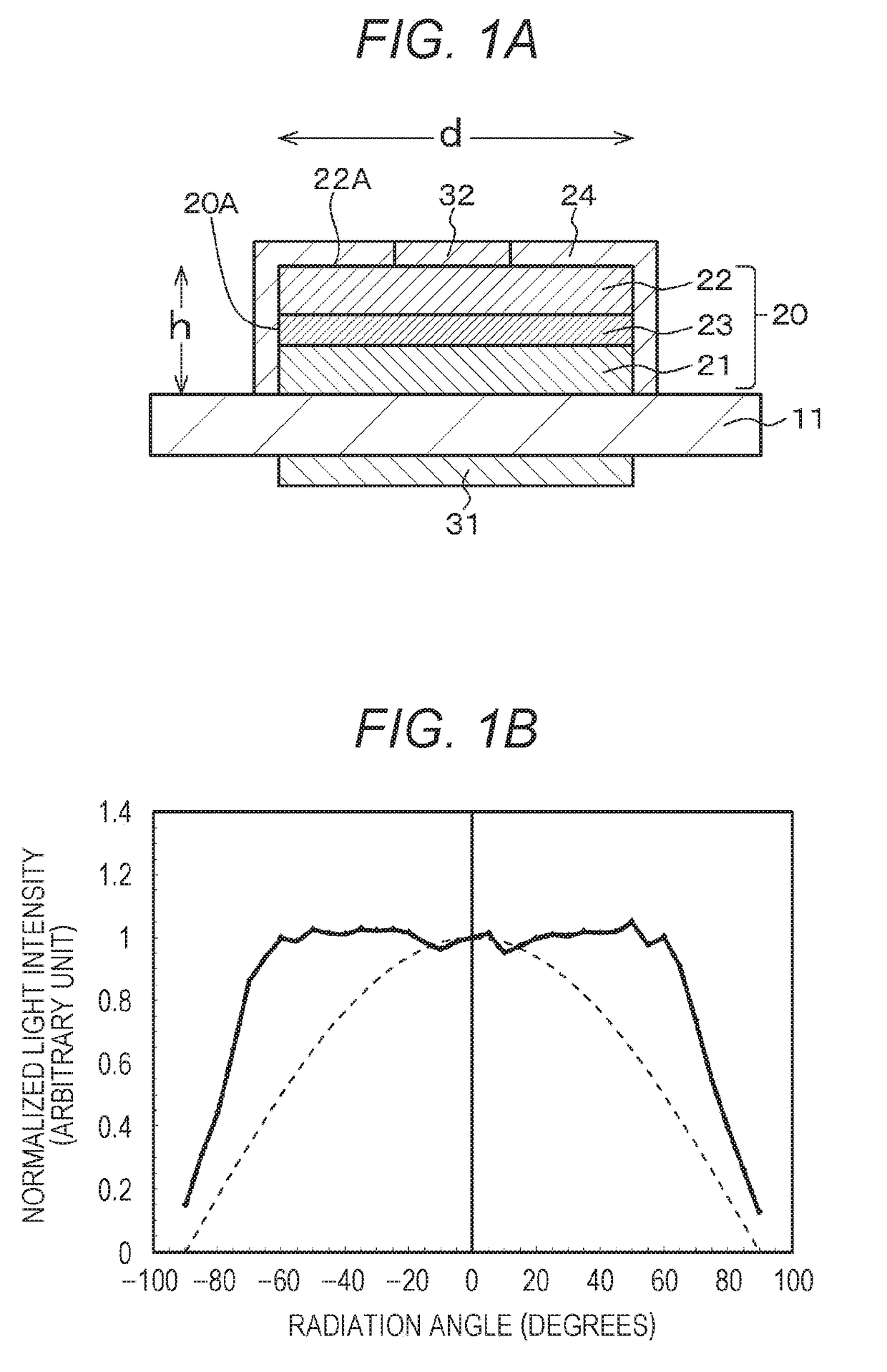
[0062]Specifically, the light-emitting element of Example 1 includes a light-emitting diode (LED) and has a constant light emission intensity over a specific range of emission angle (radiation angle) of light emitted from the center of its main light-emitting surface.

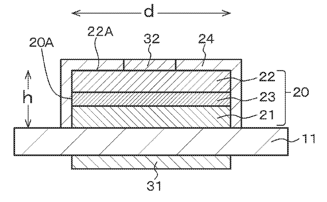
[0063]In addition, as shown in FIG. 1A, which is a schematic cross-sectional view of the light-emitting element, the light-emitting element of Example 1 has a multilayer structure 20 including a first compound semiconductor layer 21 of a first conductivity type (specifically, an n-type in the example), an active layer (light-emitting layer) 23, and a second compound semiconductor layer 22 of a second conductivity type (specifically, a p-type in the example) different from the first conductivity type. The main light-emitting surface of the light-emitting element of Example 1 includes a surface parallel ...

example 2

[0113]Example 2 is a modification of Example 1. In Example 2, the light extraction efficiency is controlled on the basis of the optical interference effect. Specifically, in Example 2, the insulating layer 24 is a transparent layer including, for example, SiO2 or SiN, which has high refractive index controllability. In addition, the thickness of a part of the insulating layer 24 on the side surface (sub light-emitting surface) 20A of the multilayer structure 20 is adjusted to increase the efficiency ηS of light extraction from the sub light-emitting surface, so that the intensity PS of light emitted from the side surface (sub light-emitting surface) 20A of the multilayer structure 20 is increased. When the thickness dIns of the insulating layer 24 satisfies formula (1):

2×nIns×dIns×cos(φ)=(k+½)×λ0  (1)

[0114]wherein dIns is the thickness of the part of the insulating layer 24 on the side surface 20A of the multilayer structure 20, nIns is the refractive index of the insulating layer 2...

example 3

[0115]Example 3 is also a modification of Example 1. In Example 3, the light extraction efficiency is controlled on the basis of the surface texture effect. Specifically, as shown in the schematic cross-sectional view of FIG. 5, the side surface 20C of the multilayer structure 20 constituting the light-emitting element is roughened to produce the surface texture effect. The roughened side surface 20C causes total reflection, which reduces the amount of light remaining in the light-emitting element, so that the efficiency (ηS) of light extraction from the side surface 20C is improved. Thus, the light emission intensity is controlled on the basis of control of the intensity of light emitted from the sub light-emitting surface. More specifically, the side surface 20C or a rough surface layer 25 is subjected to wet etching or dry etching to form surface irregularities depending on the wavelength of light, so that the efficiency (ηS) of light extraction from the side surface 20C is impro...


PUM


Abstract

The light-emitting element of the present disclosure has a constant light emission intensity over a specific range of emission angle of light emitted from the center of its main light-emitting surface.

Description

CROSS REFERENCE TO RELATED APPLICATIONS[0001]This application is a U.S. National Phase of International Patent Application No. PCT / JP2015 / 063986 filed on May 15, 2015, which claims priority benefit of Japanese Patent Application No. JP 2014-137343 filed in the Japan Patent Office on Jul. 3, 2014. Each of the above-referenced applications is hereby incorporated herein by reference in its entirety.TECHNICAL FIELD[0002]The present disclosure relates to a light-emitting element and a light-emitting element assembly.BACKGROUND ART[0003]The light emission intensity of a light-emitting element including a conventional light-emitting diode (LED) has a Lambertian distribution as shown in FIG. 8. In other words, the light emission intensity at emission angle (radiation angle) θ decreases according to cos(θ). By the way, in the process of mounting a light-emitting element on a mounting substrate using solder or other means for electrical bonding, inclination of the light-emitting element in an...

Claims


Application Information

Patent Timeline
IPC IPC(8): H01L33/20H01L33/58
CPCH01L33/20H01L33/32H01L33/30H01L33/58H01L33/46
Inventor AOYAGI, HIDEKAZUARAKIDA, TAKAHIROKAWASAKI, TAKAHIKOKOYAMA, TAKAHIROITOU, KATSUTOSHINAKASHIMA, MAKOTO
Owner SONY CORP
Why Eureka
Try Eureka