Display device and method for manufacturing the same

a technology for display devices and manufacturing methods, applied in the direction of semiconductor devices, basic electric elements, electrical apparatus, etc., can solve the problems of cracks generated in the plurality of inorganic layers, light emitting layers, and easy deterioration of light-emitting layers, so as to suppress the propagation of cracks and improve the lifespan and reliability of display devices.

Inactive Publication Date: 2017-06-08
LG DISPLAY CO LTD
View PDF4 Cites 25 Cited by
  • Summary
  • Abstract
  • Description
  • Claims
  • Application Information

AI Technical Summary

Benefits of technology

[0009]An advantage of the present disclosure is to improve lifespan and reliability of a display device by, for example, blocking a path for moisture penetration that may be formed by cracks in inorganic layers during a scribing process.
[0010]In one aspect, there is provided a display device comprising a substrate including a display area having a plurality of subpixels and a bezel area around the display area, and at least one insulating layer on the substrate and having a via hole which suppresses propagation of cracks in the bezel area.

Problems solved by technology

When a cutting process using the cutting wheel or the laser is performed, cracks may be generated in the plurality of inorganic layers.
Hence, the light emitting layer, which is vulnerable to moisture, may deteriorate.

Method used


Image

  • Display device and method for manufacturing the same
  • Display device and method for manufacturing the same
  • Display device and method for manufacturing the same

Examples


first embodiment

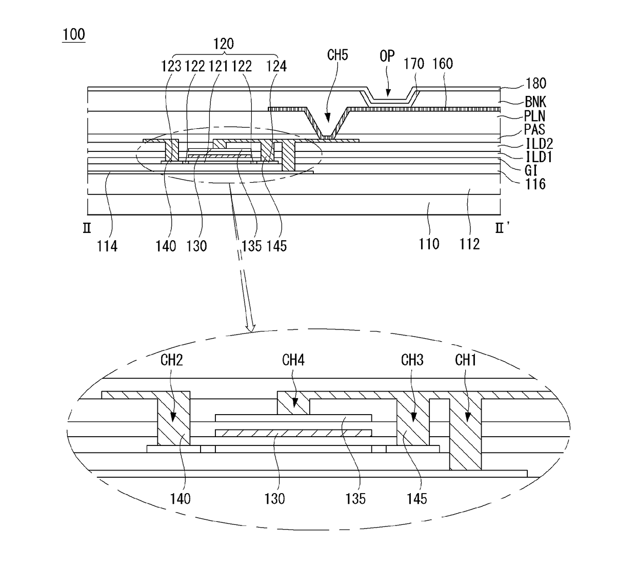
[0081]FIG. 8 is a cross-sectional view of a bezel area of an OLED display taken along II-II′ of FIG. 4. FIG. 9 is a plan view of an OLED display. FIGS. 10 and 11 are cross-sectional views of a bezel area of an OLED display taken along II-II′ of FIG. 4.

[0082]Referring to FIG. 8, in an OLED display 100 according to an embodiment of the invention, a first buffer layer 112 is positioned on a substrate 110, and a second buffer layer 116 is positioned on the first buffer layer 112. A gate insulating layer GI is positioned on the second buffer layer 116, and a first interlayer dielectric layer ILD1 and a second interlayer dielectric layer ILD2 are sequentially positioned on the gate insulating layer GI.

[0083]A passivation layer PAS is positioned on the second interlayer dielectric layer ILD2. The passivation layer PAS according to the embodiment of the invention contacts the first buffer layer 112 through at least one via hole. More specifically, the passivation layer PAS contacts the firs...

second embodiment

[0090]FIG. 12 is a cross-sectional view of a bezel area of an OLED display according to a second embodiment of the invention.

[0091]Referring to FIG. 12, a passivation layer PAS is positioned on a second interlayer dielectric layer ILD2. The passivation layer PAS according to the embodiment of the invention contacts a first buffer layer 112 through first and second via holes VIA1 and VIA2 formed by penetrating a second buffer layer 116, a gate insulating layer GI, a first interlayer dielectric layer ILD1, and the second interlayer dielectric layer ILD2. The passivation layer PAS according to the embodiment of the invention may include three openings including a first opening PAH1, a second opening PAH2, and a third opening PAH3, that are formed by partially removing the passivation layer PAS and expose the second interlayer dielectric layer ILD2 under the passivation layer PAS.

[0092]In the second embodiment of the invention, the via holes and the openings may be alternately positione...


PUM


Abstract

A display device and a method for manufacturing the same are disclosed. The display device includes a substrate including a display area having a plurality of subpixels and a bezel area around the display area; at least one insulating layer on the substrate and having a via hole which suppresses propagation of cracks in the bezel area.

Description

[0001]This application claims the priority benefit of Korean Patent Application No. 10-2015-0170514 filed on Dec. 2, 2015, which is incorporated herein by reference for all purposes as if fully set forth herein.BACKGROUND[0002]Field of the Invention[0003]The present disclosure relates to a display device and a method for manufacturing the same. More specifically, the present disclosure relates to a display device with improved lifespan and reliability and a method for manufacturing the same.[0004]Discussion of the Related Art[0005]Various display devices, which may replace cathode ray tube displays (CRTs) that are disadvantageous in terms of weight and volume, have been recently developed. Examples of such display devices include a liquid crystal display (LCD), a field emission display (FED), a plasma display panel (PDP) and an organic light emitting diode (OLED) display. An OLED display is a self-emission display device configured to emit light by exciting an organic compound. The ...

Claims


Application Information

Patent Timeline
Patent Type & Authority Applications(United States)
IPC IPC(8): H01L51/52H01L27/32
CPCH01L51/5237H01L2227/323H01L27/3258H10K59/12H10K59/123H10K59/1216H10K59/126H10K59/10H10K59/1201H10K59/124H10K50/8426H10K71/851H10K59/87H10K50/84
Inventor PARK, WONHOONRYU, WONSANGJO, DAEGYUSONG, YOUNGKYUSHIN, DONGCHAEPYO, SEUNGEUN
Owner LG DISPLAY CO LTD
Why Eureka
Try Eureka