Current Accumulative Pixel Structure for CMOS-TDI image sensor

Inactive Publication Date: 2017-06-22
TIANJIN UNIV
View PDF7 Cites 1 Cited by
  • Summary
  • Abstract
  • Description
  • Claims
  • Application Information

AI Technical Summary

Benefits of technology

[0008]The current accumulative pixel structure for CMOS-TDI image sensor is able to realize transfer the output signal of previous pixels to next pixels at exposure time, and obtained the pipelined accumulation of exposure result to the same object by the pixels of the same column. In each exposure period, output of the last line pixels is required to be read out, thus decreasing limitation of the shortest exposure time caused by read

Problems solved by technology

As a result, readout speed certainly will limit the shortest exposure period, i.e., the largest scanning frequency.
This technique however, during pipelined accumulation of pixel output signal, will introduce a gre

Method used


Image

  • Current Accumulative Pixel Structure for CMOS-TDI image sensor
  • Current Accumulative Pixel Structure for CMOS-TDI image sensor
  • Current Accumulative Pixel Structure for CMOS-TDI image sensor

Examples


Example

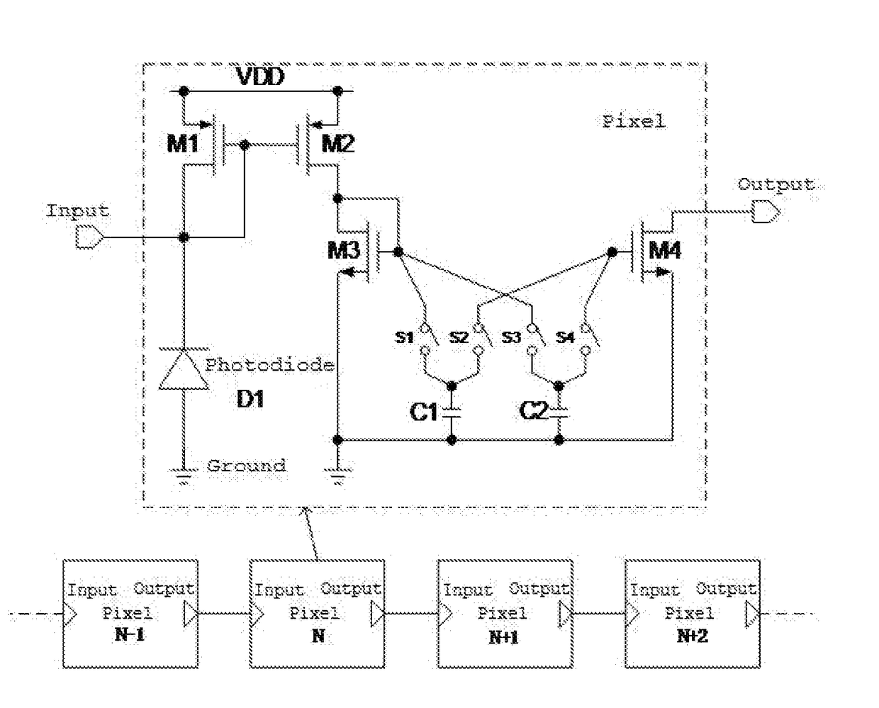
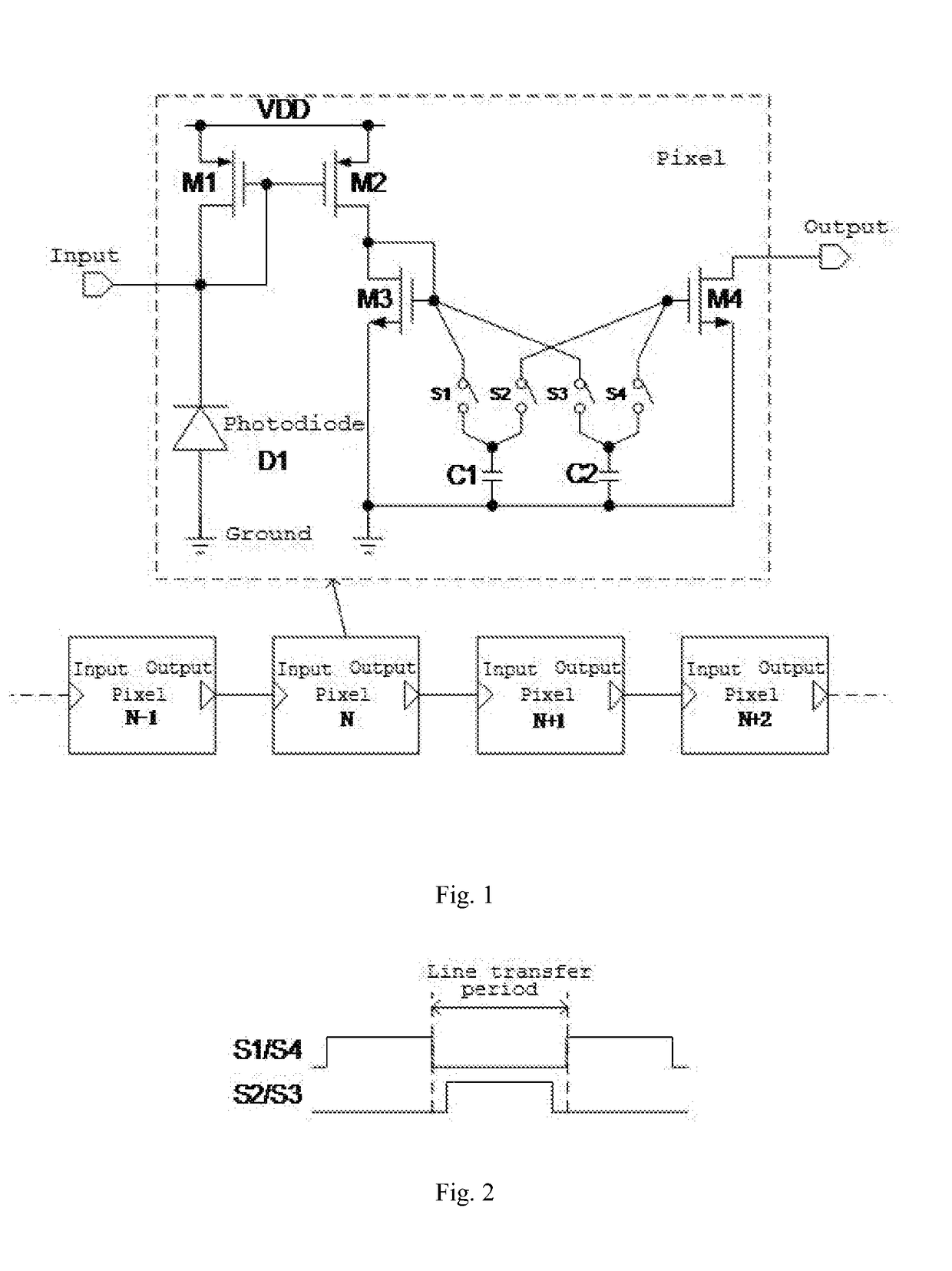
[0012]A current accumulative pixel structure for CMOS-TDI image sensor proposed by current invention is shown in FIG. 1. As shown, the pixel structure comprises a photodiode D1, four MOS transistors M1, M2, M3 and M4, four switches S1, S2, S3 and S4), and two capacitors C1, C2, the connection relationship thereof is denoted below. The anode of the photodiode D1 is connected to a ground wire, while the cathode thereof is connected to an input end. The drain and gate of the transistor M1 are both connected with the input end, while the source thereof is connected with a power source VDD. The source of the transistor M2 is connected to the power source VDD, while its gate is connected to the gate of the transistor M1, the drain of the transistor M2 is connected to both of the drain and gate of the transistor M3. The source of the transistor M3 is connected to the ground wire. Lower electrode plates of both capacitors C1 and C2 are connected to the ground wire, whereas their upper elect...


PUM


Abstract

The present invention relates to technical field of analog integrated circuit design. TDI function is better realized by CMOS image sensor and it improves scanning frequency of the CMOS-TDI image sensor and extends application range of TDI technique. To this end, the present invention proposes a technical solution of a current accumulative pixel structure for CMOS-TDI image sensor which comprises a photodiode, four MOS transistors M1, M2, M3, M4, four switches S1, S2, S3, S4, and two capacitors C1, C2; the connection relationship thereof is denoted below: the anode of the photodiode D1 is connected to a ground wire, while the cathode thereof is connected to an input end; the drain and gate of the transistor M1 are both connected with the input end, while the source thereof is connected with a power source VDD. The current invention mainly finds its application in analog integration circuit design.

Description

CROSS-REFERENCE TO RELATED APPLICATIONS[0001]This application claims priority from CN Application No. CN201410470252.0, filed Sep. 15, 2014 and PCT Application No. PCT / CN2014 / 093756, filed Dec. 12, 2014, the contents of which are incorporated herein in the entirety by reference.FIELD OF THE INVENTION[0002]The present invention relates to technical field of analog integrated circuit design and more particularly, relates to a current accumulative pixel structure for CMOS-TDI image sensor.BACKGROUND OF THE INVENTION[0003]TDI image sensor may realize higher SNR and sensitivity due to its special scanning manner and is especially suitable for high speed movement and low illumination environment. The basic principles of TDI lie in linear scanning with area pixel matrix, thus realizing exposure of the same moving object by pixels of different lines, and accumulating of exposure result of each time. This equivalently extends exposure integration time of the object, thereby greatly improving...

Claims


Application Information

Patent Timeline
IPC IPC(8): H04N5/374H04N5/378
CPCH04N5/3743H04N5/361H04N3/1525H04N5/378H04N25/768H04N25/77H04N25/771H04N25/75H04N25/63
Inventor NIE, KAIMINGYAO, SUYINGXU, JIANGTAOSHI, ZAIFENGGAO, ZHIYUANGAO, JING
Owner TIANJIN UNIV
Why Eureka
Try Eureka