Array substrate, touch display panel and touch display device

Inactive Publication Date: 2017-07-06
SHANGHAI AVIC OPTOELECTRONICS +1
View PDF5 Cites 11 Cited by
  • Summary
  • Abstract
  • Description
  • Claims
  • Application Information

AI Technical Summary

Benefits of technology

The present patent provides a solution to prevent data lines from being interfered by touch signal lines due to increased capacitance between them. This is achieved by placing a driver chip and multiple first connection lines in the non-display region of the array substrate, while keeping the touch signal lines away from the first connection lines. This reduces the likelihood of electrostatic discharge and helps prevent open or short circuits. In summary, the technical effect of this solution is to improve the reliability and stability of the touch display device.

Problems solved by technology

Also, since the touch signal lines and data lines are overlapped with each other in the direction perpendicular to the substrate, a capacitance between the touch signal lines and the data lines would be increased, thus causing the problem of generating electrostatic discharge and open circuit or short circuit due to the release of the electrostatic discharge, etc.
In the non-display region, the plurality of touch signal lines are not overlapped with the plurality of first connection lines in a direction perpendicular to the substrate, so that the capacitance between the touch signal lines and the first connection lines is decreased, thus reducing the possibilities of the generation of electrostatic discharge and the open or short circuit due to the release of electrostatic discharge.

Method used


Image

  • Array substrate, touch display panel and touch display device
  • Array substrate, touch display panel and touch display device
  • Array substrate, touch display panel and touch display device

Examples


Embodiment Construction

[0020]Below in conjunction with the accompanying drawings and the embodiment of the present disclosure will be further described in detail. To be understood that the specific embodiments described herein merely illustrate the disclosure and not limiting of the present invention. It also is noted that, for ease of description, the drawings illustrate only with the present disclosure is related to some but not all content.

[0021]An embodiment of the present disclosure provides an array substrate.

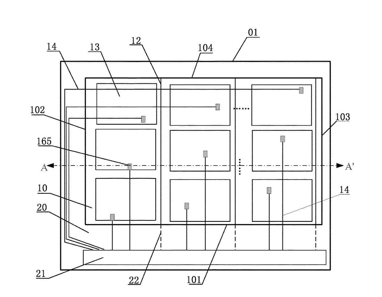
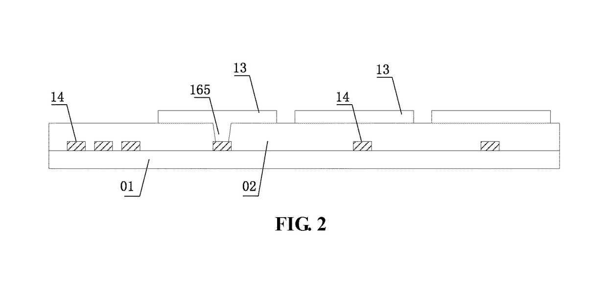
[0022]FIG. 1 is a schematic plan view showing an embodiment of a structure of an array substrate according to an embodiment of the present disclosure. As shown in FIG. 1, the array substrate comprises: a substrate 01; a display region 10 and a non-display region 20 surrounding the display region 10, the non-display region 20 is provided with a driver chip 21. The display region 10 includes: a plurality of data lines 12, and each of the plurality of data lines 12 is electrically connected to the...


PUM


Abstract

The present disclosure discloses an array substrate, touch display panel and touch display device. The array substrate comprises a substrate, a display region and a non-display region surrounding the display region. A driver chip is provided in the non-display region. The display region comprises a plurality of data lines. Each of the plurality of data lines is electrically connected to the driver chip via a respective one of a plurality of first connection lines; and a plurality of touch electrode blocks. The plurality of touch electrode blocks are electrically connected to the driver chip via a plurality of touch signal lines. In the non-display region, the plurality of touch signal lines are not overlapped with the plurality of first connection lines in a direction perpendicular to the substrate.

Description

CROSS-REFERENCES TO RELATED APPLICATIONS[0001]This application claims priority to a Chinese patent application No. 201511027131.X filed on Dec. 31, 2015 and entitled “Array Substrate, Touch Display Panel and Touch Display Device”, the disclosure of which is incorporated herein by reference in its entirety.TECHNICAL FIELD[0002]The present disclosure relates to the field of display technology, in particular to an array substrate, a touch panel display and a touch display device.TECHNICAL BACKGROUND[0003]With the rapid development of display technology, the touch screen has been populated in people lives. Compared to a conventional display device which only provides the display function, the display device using the touch screen enables the user to make information interaction with the display control host. The display device with a touch function not only can perform a display function, but also can perform a controlled function by touch operation.[0004]Currently the display device ha...

Claims


Application Information

Patent Timeline
IPC IPC(8): G06F3/044G06F3/041
CPCG06F3/0412G06F3/044G06F3/0416G09G3/20G06F3/04164G06F3/0443
Inventor XI, KERUICUI, TINGTINGXIE, ZHENGFANG
Owner SHANGHAI AVIC OPTOELECTRONICS
Why Eureka
Try Eureka