Radiation detector assembly

a radiation detector and assembly technology, applied in the direction of x/gamma/cosmic radiation measurement, instruments, radioation controlled devices, etc., can solve the problems of difficult or impractical implementation in practice, high cost and small panel size, and limitations in the practical size of silicon wafers

Active Publication Date: 2017-07-06
GENERAL ELECTRIC CO
View PDF8 Cites 7 Cited by
  • Summary
  • Abstract
  • Description
  • Claims
  • Application Information

AI Technical Summary

Benefits of technology

This patent describes a radiation detector that includes a substrate and a tiled array of complementary metal-oxide-semiconductor (CMOS) tiles positioned on the substrate. The CMOS tiles have a plurality of contact pads that are connected to a plurality of conductive traces on the substrate using conductive bridges. The detector also includes an optically transparent layer with conductive traces that are positioned over the CMOS tiles opposite the substrate. The technical effects of this patent include improved detection of radiation and more precise positioning of the CMOS tiles, which leads to better performance and reliability of the detector.

Problems solved by technology

Despite this, the mainstream technology for fabricating X-ray panels for medical and industrial inspection utilizes amorphous silicon TFTs due to their competitive cost and large area capability.
However, disadvantages of using c-Si include: higher cost and smaller panel size due to limitations in the practical size of silicon wafers used to fabricate c-Si devices.
Such wafer size limitations may require tiling multiple, smaller panels together to form a detector panel of useful size.
However, such tiling arrangements introduce complexities in the electrical interconnection arrangements needed to operate (e.g., readout) such a detector panel and may be difficult or impractical to implement in practice.

Method used


Image

  • Radiation detector assembly
  • Radiation detector assembly
  • Radiation detector assembly

Examples


Embodiment Construction

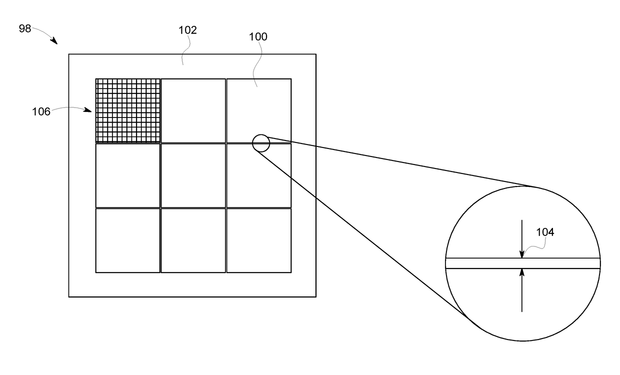
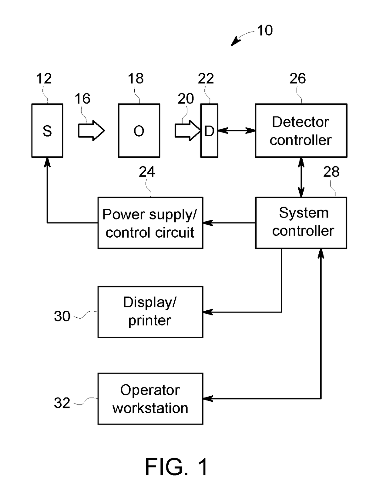
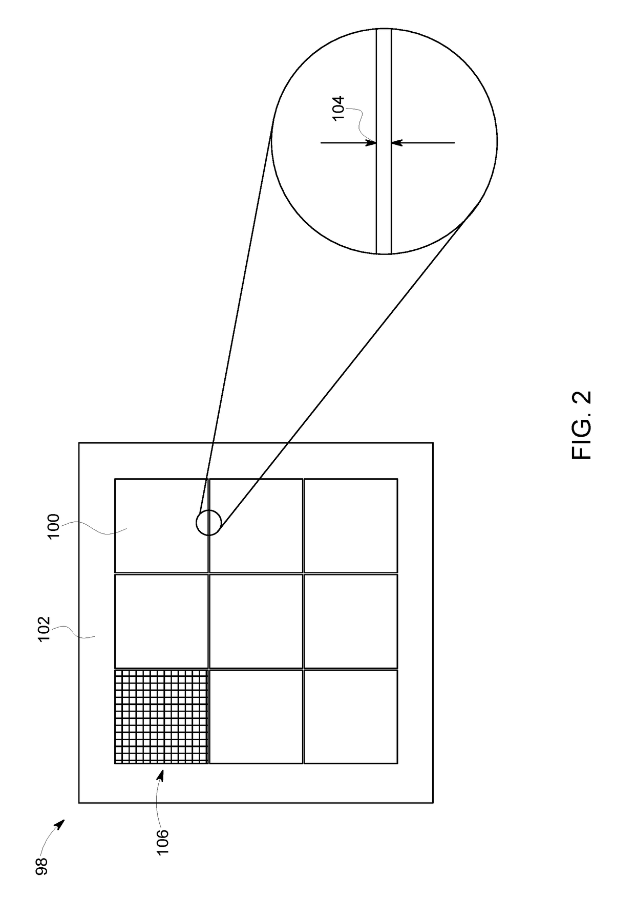
[0022]One or more specific implementations will be described below. In an effort to provide a concise description of these implementations, not all features of an actual implementation are described in the specification. It should be appreciated that in the development of any such actual implementation, as in any engineering or design project, numerous implementation-specific decisions must be made to achieve the developers' specific goals, such as compliance with system-related and business-related constraints, which may vary from one implementation to another. Moreover, it should be appreciated that such a development effort might be complex and time consuming, but would nevertheless be a routine undertaking of design, fabrication, and manufacture for those of ordinary skill having the benefit of this disclosure

[0023]While the following discussion is generally provided in the context of medical imaging, it should be appreciated that the present techniques are not limited to such m...


PUM


Abstract

Various approaches are discussed for using four-side buttable CMOS tiles to fabricate detector panels, including large-area detector panels. Fabrication may utilize pads and interconnect structures formed on the top or bottom of the CMOS tiles. Electrical connection and readout may utilize readout and digitization circuitry provided on the CMOS tiles themselves such that readout of groups or sub-arrays of pixels occurs at the tile level, while tiles are then readout at the detector level such that readout operations are tiered or multi-level.

Description

BACKGROUND[0001]The subject matter disclosed herein relates to the fabrication and use of radiation detectors, including X-ray radiation detectors composed of arrays of CMOS tiles.[0002]Non-invasive imaging technologies allow images of the internal structures or features of a subject (patient, manufactured good, baggage, package, or passenger) to be obtained non-invasively. In particular, such non-invasive imaging technologies rely on various physical principles, such as the differential transmission of X-rays through the target volume or the reflection of acoustic waves, to acquire data and to construct images or otherwise represent the internal features of the subject.[0003]By way of example, digital X-ray imaging systems are used to generate digital data in a non-invasive manner and to reconstruct such digital data into useful radiographic images. In current digital X-ray imaging systems, radiation from a source is directed toward a subject or object, typically a patient in a med...

Claims


Application Information

Patent Timeline
Patent Type & Authority Applications(United States)
IPC IPC(8): H01L27/146G01T1/24G01T1/20
CPCH01L27/14636H01L27/14658G01T1/247G01T1/2018H01L27/14689H01L27/14625H01L27/14661H01L27/14663H01L27/1469
Inventor JACOB, BIJUVAFI, HABIBYANOFF, BRIAN DAVIDSHAW, JEFFERY JONGUO, JIANJUN
Owner GENERAL ELECTRIC CO
Why Eureka
Try Eureka