Drive unit of semiconductor element

a technology of drive unit and semiconductor element, which is applied in the direction of transistors, electronic switching, pulse techniques, etc., can solve the problems of delay in gate voltage rise and increase in turn-on loss, and achieve the effect of increasing turn-on loss

Active Publication Date: 2017-07-06
FUJI ELECTRIC CO LTD
View PDF2 Cites 6 Cited by
  • Summary
  • Abstract
  • Description
  • Claims
  • Application Information

AI Technical Summary

Benefits of technology

[0006]However, in the conventional example described in WO 2013-157086 A1, the clamp circuit is configured by the series circuit of the diode and the capacitor, and an anode of the diode is connected to the gate of the IGBT. Thus, there are problems in that a charge voltage to the capacitor cannot be charged to only a voltage lower by...

Problems solved by technology

Thus, there are problems in that a charge voltage to the capacitor cannot be charged to only a voltage lower by a drop voltage in the diode, a range of an accumulation voltage is narrowed, and a reverse recovery surge voltag...

Method used


Image

  • Drive unit of semiconductor element
  • Drive unit of semiconductor element
  • Drive unit of semiconductor element

Examples


Embodiment Construction

[0017]Next, one exemplary embodiment of the present invention will be described with reference to the drawings. In the following description of the drawings, the same or similar portions are denoted by the same or similar reference numerals.

[0018]In addition, the following exemplary embodiment illustrates devices and methods to embody the technical idea of the present invention, and the technical idea of the present invention does not limit the material, shape, structure, arrangement, and the like of a component to those described below. Various changes can be added to the technical idea of the present invention within the technical scope defined by claims.

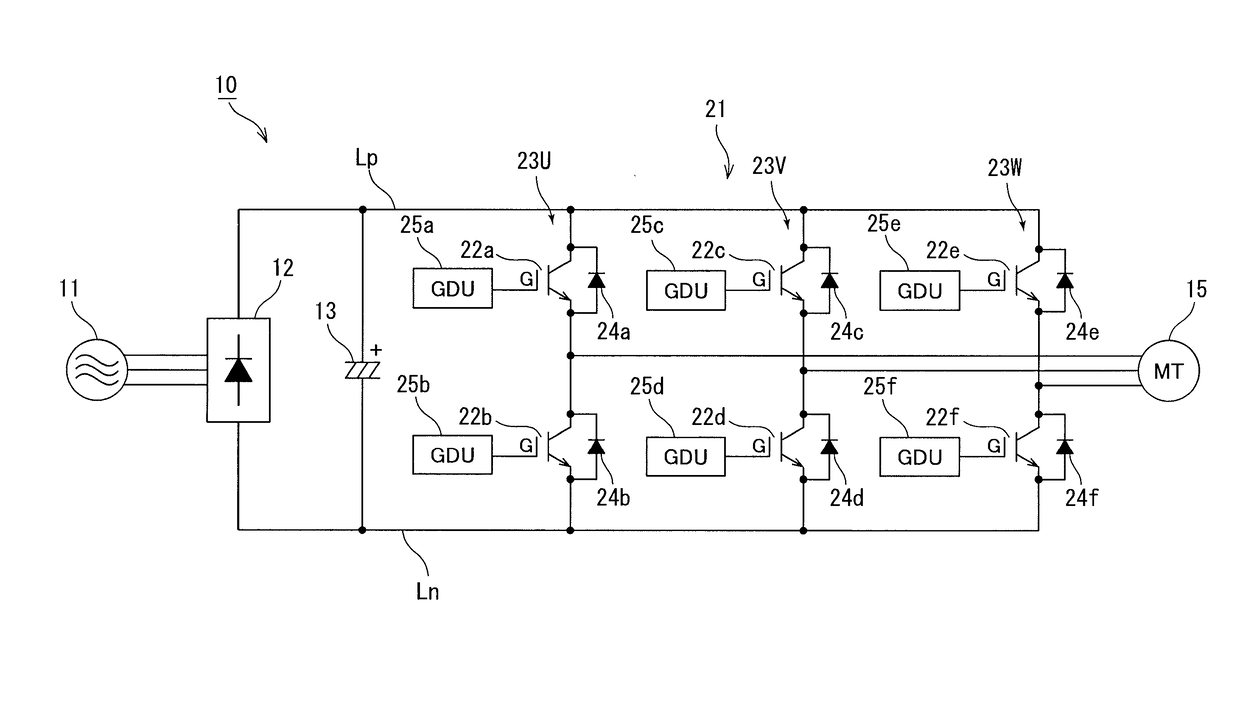
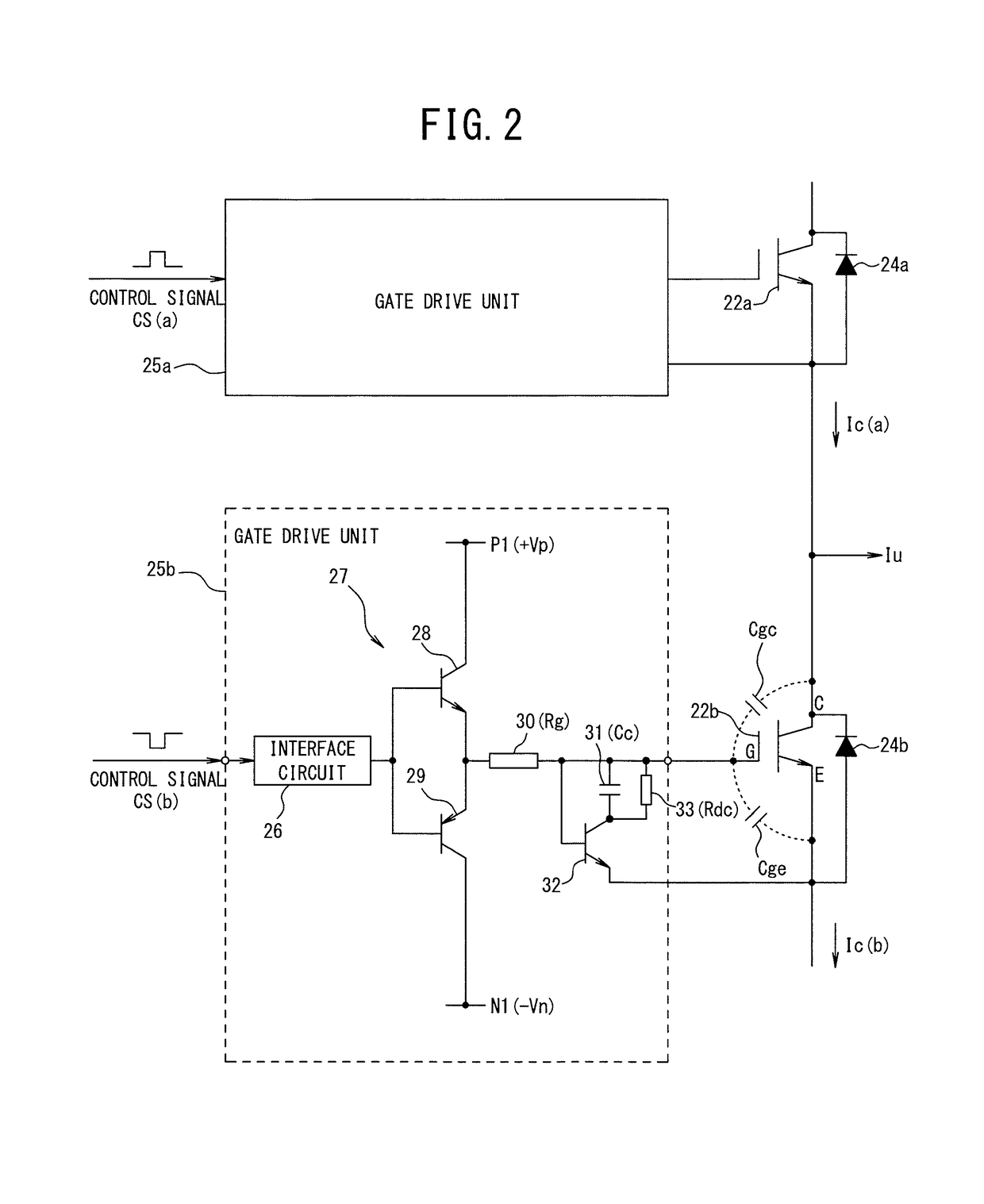
[0019]Hereinafter, a drive unit of a semiconductor element according to one exemplary embodiment of the present invention will be described with reference to the drawings. The present exemplary embodiment is described by taking a voltage drive semiconductor element as the semiconductor element and a gate drive unit of a semiconduc...


PUM


Abstract

A drive unit of a semiconductor element including: a drive circuit for driving a control electrode of a voltage control semiconductor element to which a freewheeling diode is connected in anti-parallel; a resistor connected between the control electrode and the drive circuit; a capacitor having one terminal connected between the resistor and the control electrode; and a switch element connected between another terminal of the capacitor and a low-voltage-side electrode of the voltage control semiconductor element, wherein a control electrode of the switch element is connected to a connection point of the resistor and the capacitor.

Description

CROSS REFERENCE TO RELATED APPLICATIONS AND INCORPORATION BY REFERENCE[0001]This application claims benefit of priority under 35 USC 119 based on Japanese Patent Application No. 2016-000627 filed on Jan. 5, 2016, the entire contents of which are incorporated by reference herein.TECHNICAL FIELD[0002]The present invention relates to a drive unit of a semiconductor element, which is applied to a power converter or the like.BACKGROUND ART[0003]Conventionally, a power converter using an IGBT (Insulated Gate Bipolar Transistor) that is a voltage drive semiconductor element is known (for example, WO 2013-157086 A1). In such a power converter, a switching arm is usually configured by serially connecting two IGBTs.[0004]In each of the two IGBTs that configure the switching arm, in order to suppress increase of a current flowing in the IGBTs when the IGBTs become on states at the same time, a clamp circuit configured by a series circuit of a diode and a capacitor is connected to between a gat...

Claims


Application Information

Patent Timeline
IPC IPC(8): H03K17/082H02P27/08H01L27/02
CPCH03K17/0826H01L27/0255H01L27/0285H02P27/08H01L27/0288H01L27/0292H01L27/0259H03K17/0406H03K17/0412H03K17/162H03K17/168H03K2217/0036
Inventor CHEN, SHUANGCHINGOGAWA, SHOGO
Owner FUJI ELECTRIC CO LTD
Why Eureka
Try Eureka