Semiconductor device

a technology of semiconductor devices and drain electrodes, applied in the direction of semiconductor devices, semiconductor/solid-state device details, electrical apparatus, etc., can solve the problems of not only effectively inhibiting the reaction between aluminum electrodes, the spread resistance is not easily reduced, and the overall thickness of the common drain electrode is increased, so as to reduce the spread resistance of the semiconductor device during operation, reduce the common drain electrode common resistance, and reduce the overall thickness of the common drain electrod

Inactive Publication Date: 2017-07-20
UBIQ SEMICON
View PDF8 Cites 7 Cited by
  • Summary
  • Abstract
  • Description
  • Claims
  • Application Information

AI Technical Summary

Benefits of technology

[0014]In view of the above, the present invention provides a semiconductor device capable of effectively solving the above-described problems encountered in the prior art by reducing the amount of warping of the semiconductor substrate when the temperature of the semiconductor substrate is changed.
[0022](1) It is possible to increase the area of the barrier film by arranging the peripheral edge of the barrier film more outwardly than the peripheral edge of the opening portion, and not only to reduce the spreading resistance of the respective electrodes. The amount of metal on the first surface side of the semiconductor substrate is increased and the difference between the amounts of the metal on the second surface side covered by the common drain electrode can be reduced. Therefore, the amount of metal formed on the front surface and the back surface of the semiconductor substrate can effectively reduce the amount of warping to the semiconductor substrate when it is affected by temperature change.
[0024](3) The common drain electrode may be covered by a metal film formed by the same kind of metal as the barrier film, thereby increasing the overall thickness of the common drain electrode to reduce the common resistance of the common drain electrode.
[0025](4) The first source electrode and the second source electrode may be formed by surrounding the first gate electrode and the second gate electrode, respectively, and area of the first source electrode and the second source electrode is increased in order to reduce the spreading resistance of the semiconductor device during operation.
[0026](5) The source electrode may be covered only by an insulating layer made of an inorganic insulating film or a resin insulating film, so that the number of components of the semiconductor device and the manufacturing steps can be reduced.

Problems solved by technology

The formation of the metal layer under the bump can not only effectively inhibit the reaction between the aluminum electrode and solder, but also improve the solder wettability.
However, when the semiconductor device described in the above-mentioned patent document is put into operation, it is likely to encounter a problem that the spreading resistance is not easily reduced.
However, since the cross-sectional areas of the source electrodes 114 and 116 in the direction of the current flow cannot be increased, the spreading resistance cannot be effectively reduced.

Method used


Image

  • Semiconductor device
  • Semiconductor device
  • Semiconductor device

Examples


Embodiment Construction

[0041]Hereinafter, a semiconductor device according to a preferred embodiment of the present invention will be described in detail based on the drawings. In the following description, the same reference numerals will be used for like components, and redundant descriptions of parts thereof will be omitted.

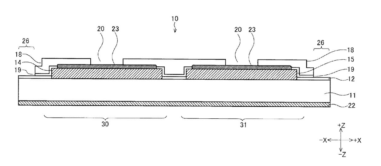
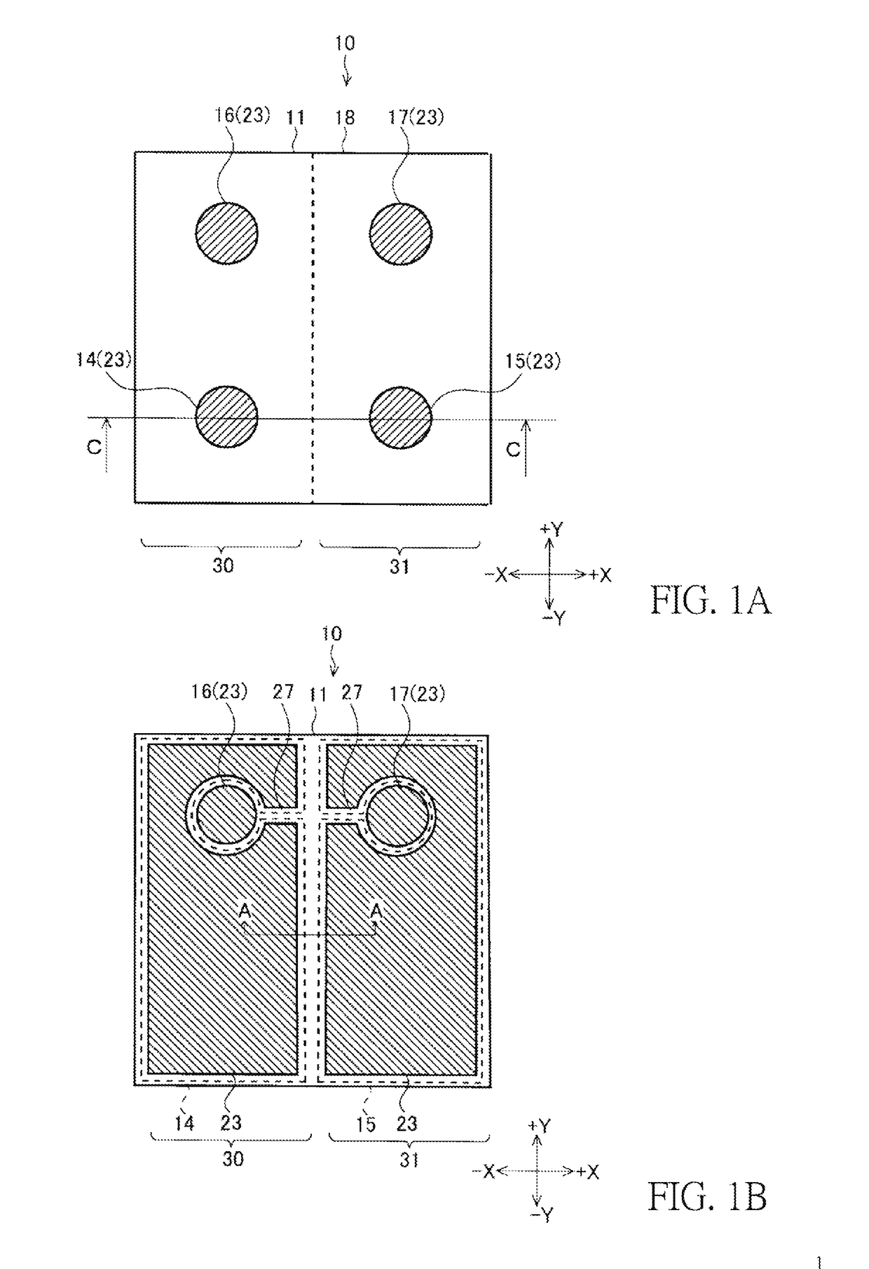
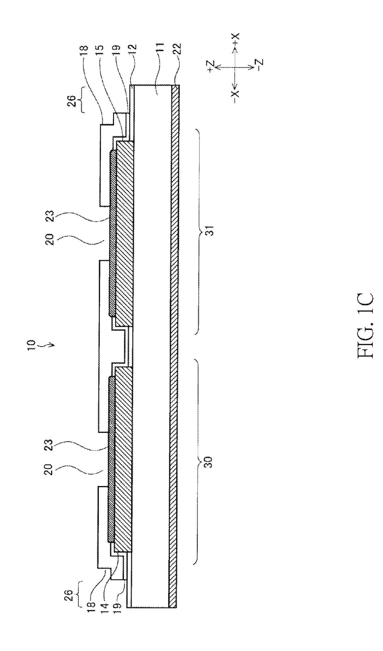
[0042]Please refer to FIGS. 1A to 1C. FIG. 1A illustrates a top view of the semiconductor device 10, and FIG. 1B shows a top view of the respective electrode structures formed in the semiconductor device 10. FIG. 1C shows a cross section taken along the CC line in FIG. 1A.

[0043]As shown in FIG. 1A, the semiconductor device 10 is a small-sized semiconductor device using a Wafer Level Package (WLP), and a plurality of electrodes connected to an active area formed on the semiconductor substrate 11. The semiconductor substrate 11 has a rectangular shape in which the side length in the Y direction is longer than the side length in the X direction. A first transistor 30 is formed on the −...


PUM


Abstract

A semiconductor device is disclosed. The semiconductor device includes a semiconductor substrate having an active area and a source electrode formed on the semiconductor substrate. The source electrode is covered by a hard passivation layer and an opening is formed in the hard passivation layer. An under bump metal (UBM) layer used as a barrier film is formed broader than the opening to reduce a spreading resistance during the operation of the semiconductor device and a warp amount of the semiconductor substrate caused by variation of temperature.

Description

BACKGROUND[0001]1. Technical Field[0002]The present invention relates to a semiconductor device, and more particularly to a semiconductor device in which a plurality of Metal-Oxide-Semiconductor Field-Effect Transistors (MOSFETs) are integrated on a semiconductor substrate.[0003]2. Description of the Related Art[0004]As semiconductor devices have been widely used in various portable devices such as mobile phones, smart phones, notebook computers, and tablet computers, there has been a demand for a compact, thin and light-weight semiconductor device, Chip scale package (Chip Scale Package, CSP) of the semiconductor device.[0005]In a typical wafer-level package, an active region is formed in the vicinity of a surface of a semiconductor device such that an electrode connected to the active region is formed on a semiconductor substrate, and the wafer-level encapsulation body is passed through a solder electrode soldered to the electrode to allow packaging on a package substrate in a Fli...

Claims


Application Information

Patent Timeline
Patent Type & Authority Applications(United States)
IPC IPC(8): H01L23/00H01L29/78H01L27/088H01L23/535
CPCH01L23/562H01L24/05H01L23/535H01L29/7813H01L27/088H01L24/03H01L2924/3511H01L2224/03464H01L2224/05155H01L2224/05144H01L2224/05164H01L2224/0391H01L2224/0401H01L23/3171H01L24/11H01L24/14H01L2224/1414H01L2224/14141H01L2224/141H01L2924/01028H01L2924/01079H01L23/3192H01L21/823487H01L2224/0615H01L24/06H01L2224/04026H01L2224/05553H01L2224/05555H01L2224/05567H01L2224/05644H01L2224/05664H01L2224/06051H01L2224/06181H01L2224/94H01L24/13H01L24/94H01L2224/0348H01L2924/00015H01L2924/13091H01L2224/05022H01L2224/05124H01L2224/131H01L2224/05073H01L2224/05082H01L2924/00014H01L21/563H01L2224/73204H01L2224/03H01L2924/014H01L23/3114H01L23/485H01L21/76841H01L29/78
Inventor ARAI, HIROKIKOYANO, MASASHIMATSUURA, NOBUYOSHI
Owner UBIQ SEMICON
Why Eureka
Try Eureka