3D semiconductor device and structure

a semiconductor and integrated circuit technology, applied in semiconductor devices, semiconductor/solid-state device details, instruments, etc., can solve the problems of destroying the lattice structure of the doped layer, reducing the performance of the wire (interconnect) that connects the transistors together, and requiring a long time of thermal treatment at very high temperatur

Active Publication Date: 2017-07-27
MONOLITHIC 3D
View PDF8 Cites 60 Cited by
  • Summary
  • Abstract
  • Description
  • Claims
  • Application Information

AI Technical Summary

Benefits of technology

[0022]In one aspect, a 3D integrated circuit device, comprising: a first layer comprising first transistors, overlaid by a second layer comprising second transistors, overlaid by a third layer comprising third transistors, wherein said first layer, said second layer and said third layer are each thinner than 2 microns, wherein said first layer comprises first circuits comprising at least one of said first transistors, wherein said second layer comprises second circuits comprising at least one of said second transistors, and wherein said third layer comprises a charge pump circuit and control circuits to control said first circuits and said second circuits.
[0023]In another aspect, a 3D integrated circuit device, comprising: a first layer comprising first transistors, overlaid by a second layer comprising second transistors, overlaid by a third layer comprising third transistors, wherein said first layer, said second layer and said third layer are each thinner than 2 microns, wherein said first layer

Problems solved by technology

However, wires (interconnects) that connect together transistors degrade in performance with “scaling”.
But this exfoliating implant method can destroy lattice structure of the doped layer 400 by heavy ion-implanting.
In this case, to recover the destroyed lattice structure, a long time thermal treatment in very high temperature is required.
This method has a critical disadvantage which can destroy lattice structures of the substrate because it uses high amount of ion implantation.
However, it is not designed for 3D IC either.
Such high temperature processing certainly destroys underlying devices and interconnect layers.
It seems that there is no way to cure the lattice damage at low tem

Method used


Image

  • 3D semiconductor device and structure
  • 3D semiconductor device and structure
  • 3D semiconductor device and structure

Examples


Embodiment Construction

[0052]An embodiment of the invention is now described with reference to the drawing figures. Persons of ordinary skill in the art will appreciate that the description and figures illustrate rather than limit the invention and that in general the figures are not drawn to scale for clarity of presentation. Such skilled persons will also realize that many more embodiments are possible by applying the inventive principles contained herein and that such embodiments fall within the scope of the invention which is not to be limited except by the appended claims.

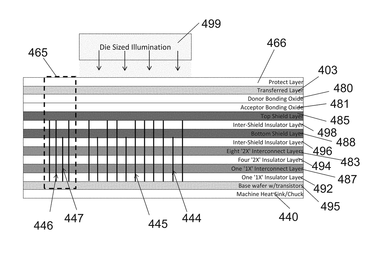
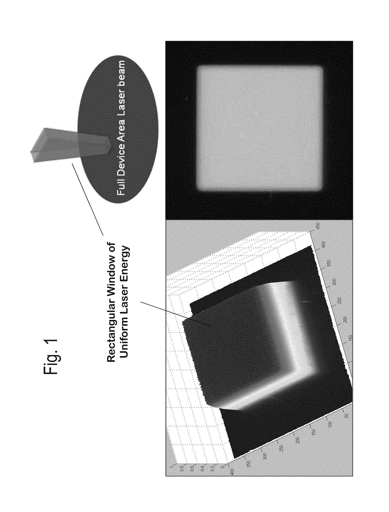
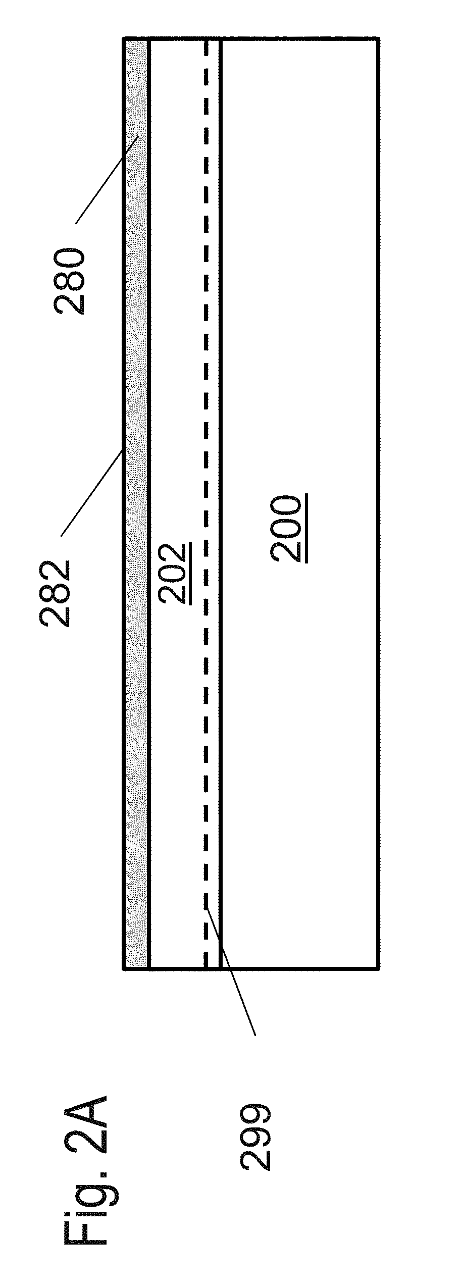
[0053]Some drawing figures may describe process flows for building devices. The process flows, which may be a sequence of steps for building a device, may have many structures, numerals and labels that may be common between two or more adjacent steps. In such cases, some labels, numerals and structures used for a certain step's figure may have been described in the previous steps' figures.

[0054]Some monolithic 3D approaches are desc...


PUM


Abstract

A 3D integrated circuit device, including: a first layer including first transistors, overlaid by a second layer including second transistors, overlaid by a third layer including third transistors, where the first layer, the second layer and the third layer are each thinner than 2 microns, where the first layer includes first circuits including at least one of the first transistors, where the second layer includes second circuits including at least one of the second transistors, and where the third layer includes a charge pump circuit and control circuits to control the first circuits and the second circuits

Description

[0001]This application is a continuation-in-part of co-pending U.S. patent application Ser. No. 14 / 607,077 filed on Jan. 28, 2015; which claims benefit of provisional U.S. Patent Application No. 62 / 042,229, filed on Aug. 26, 2014, provisional U.S. Patent Application No. 62 / 035,565, filed on Aug. 11, 2014, provisional U.S. Patent Application No. 62 / 022,498, filed on Jul. 9, 2014, and provisional U.S. Patent Application No. 61 / 932,617, filed on Jan. 28, 2014. The contents of the foregoing applications are incorporated herein by reference.BACKGROUND OF THE INVENTION[0002]1. Field of the Invention[0003]This application relates to the general field of Integrated Circuit (IC) devices and fabrication methods, and more particularly to multilayer or Three Dimensional Integrated Circuit (3D-IC) devices and fabrication methods.[0004]2. Discussion of Background Art[0005]Over the past 40 years, there has been a dramatic increase in functionality and performance of Integrated Circuits (ICs). This...

Claims


Application Information

Patent Timeline
IPC IPC(8): H01L27/06H01L27/108H01L29/161H01L29/78G11C5/14H01L21/8234H01L21/683H01L23/528H01L23/522H01L21/762H01L23/552H01L23/367H01L27/24G11C5/02H01L27/02
CPCH01L27/0688H01L2221/68363H01L27/10805H01L27/10897H01L29/161H01L27/0251H01L29/7827G11C5/147H01L21/823475H01L21/6835H01L23/528H01L23/5226H01L21/76251H01L23/552H01L23/367H01L27/10847H01L27/2481H01L27/2454G11C5/145G11C5/02H01L2221/68345H01L27/0222H01L21/8221H01L21/823871H01L23/481H01L23/49827H01L23/50H01L27/0694H01L27/088H01L27/092H01L2224/48091H01L2924/3025H01L2924/00014H01L29/66545H01L29/66628H01L21/76254H01L27/0924H01L2924/14H01L2224/04042H01L24/05H01L24/48H01L2924/13091H01L27/0922H01L21/823842H10B12/34H01L2224/45099H01L2224/05599H01L2924/00H01L21/48H01L23/488
Inventor OR-BACH, ZVICRONQUIST, BRIAN
Owner MONOLITHIC 3D
Why Eureka
Try Eureka