This helps you quickly interpret patents by identifying the three key elements:
Problems solved by technology
Method used
Benefits of technology
Benefits of technology
[0139]In FIG. 7A, the conductive layer 71, the conductive layer 72, and the conductive layer 73 can be formed using a conductive material that blocks visible light. For example, a conductive material including a metal or an alloy can be used. In this case, the electrical resistances of the conductive layer 71, the conductive layer 72, and the conductive layer 73 can be significantly reduced as compared with the case of using a material having a light-transmitting property. Thus, the conductive layer 71 and the like can have a small thickness, and various advantageous effects are obtained such as a reduction in the stress that is applied to the conductive layer 71 and the like and a reduction in the thickness of the display device 10. Furthermore, the conductivity of the conductive layer 71 and the like is increased, so that the area of a display region can be enlarged.
[0140]In the example shown in FIG. 7B, the light-blocking layer 66 and the insulating layer 41 are provided in a position closer to the substrate 12 side than the conductive layer 71 and the like. In such a structure, the conductive layer 71, the conductive layer 72, and the conductive layer 73 can be close to the neutral plane of the display device 10. Thus, stress that is applied by deformation such as bending of the display device 10 can be relieved even in the case where the conductive layer 71, the conductive layer 72, and the conductive layer 73 are formed using a material with a high Young's modulus.
[0141]Furthermore, because the light-blocking layer 66 is provided closer to the substrate 12 side than the conductive layer 71 and the like and covers the conductive layer 71 and the like, external light does not reach the conductive layer 71 and the like, and reflection of external light by the conductive layer 71 and the like can be prevented. Thus, the visibility of the display device can be increased.
[0142]In the example, the barrier layer 22 is preferably formed using a material with a higher Young's modulus than at least one or more of the light-blocking layer 66, the insulating layer 40, the insulating layer 41, the insulating layer 42, the insulating layer 43, the adhesive layer 17, and the substrate 12.
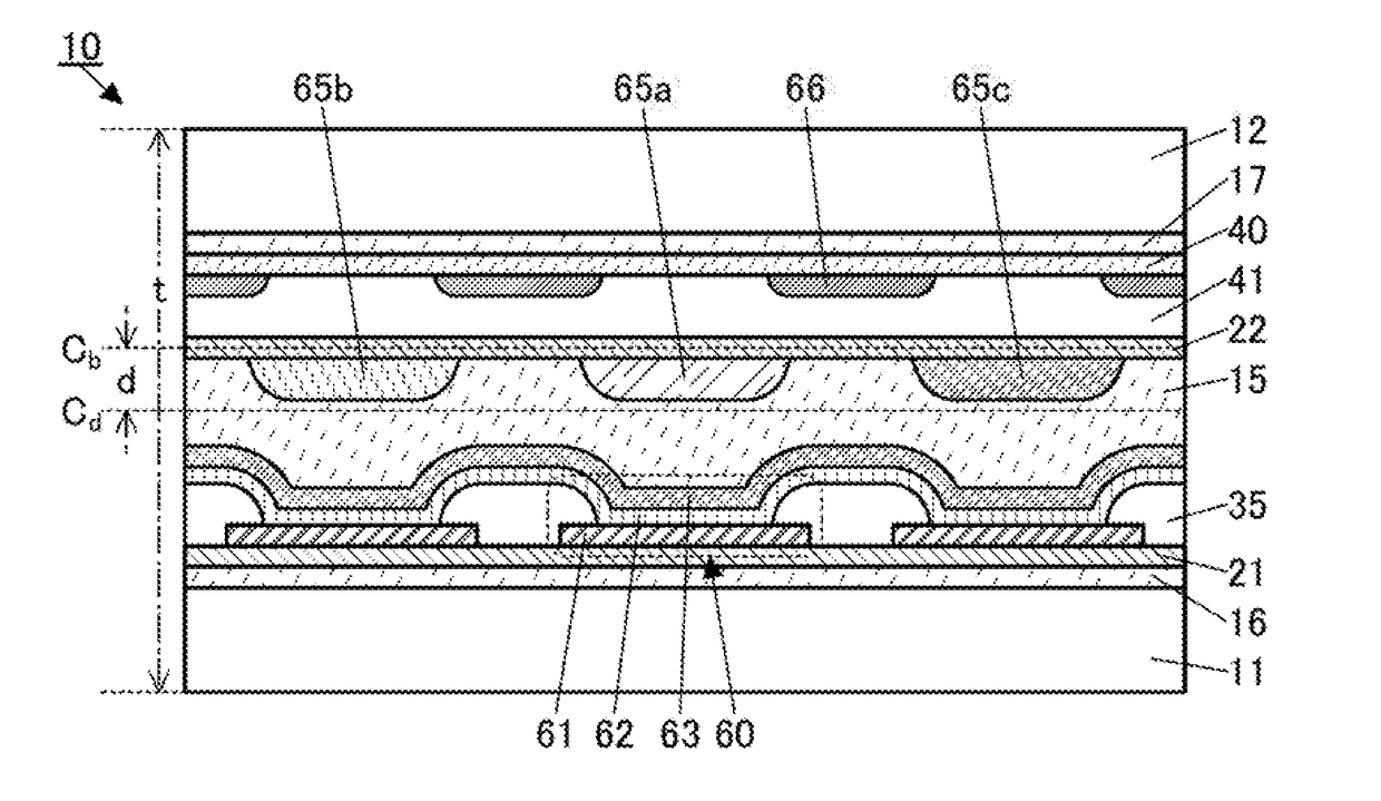
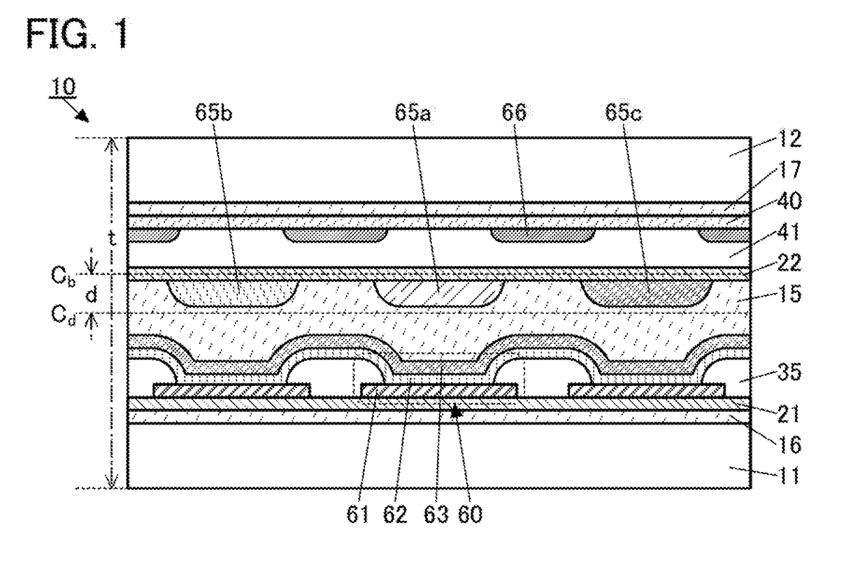
[0143]In FIGS. 7A and 7B, the positional relation between the coloring layer 65a, the coloring layer 65b, and the barrier layer 22, the structure of the display element 60, and the like are similar to those in Cross-sectional structure
Problems solved by technology
It is difficult to enhance the moisture resistance of the flexible substrate, and therefore, the above-described barrier layer is essential.
However, in some cases, a material having a high barrier property is cracked by the stress applied to the material by deformation such as bending of the flexible device, which significantly impairs the barrier property of the material.
Method used
Image
Click on the blue label to locate the original text in one second.
Reading with bidirectional positioning of images and text.
Examples
embodiment 1
[0061]This embodiment describes structure examples and a manufacturing method example of a display device (a display panel) that is given as an example of a flexible device of one embodiment of the present invention.
[0062]One embodiment of the present invention includes a plurality of display elements, a light-blocking layer, an adhesive layer, and a barrier layer between a pair of substrates. The pair of substrates is also referred to as first substrate and second substrate in some cases. The display elements are between the first substrate and the adhesive layer. The light-blocking layer is between the second substrate and the adhesive layer.
[0063]Typical examples of the display element include a light-emitting element such as an organic EL element (organic light-emitting diode (OLED)) or a quantum-dot light-emitting diode (QLED). Furthermore, a light-emitting diode (LED) may be used.
[0064]Other examples of the display element include a liquid crystal element, a micro electro mech...
example 3
Cross-Sectional Structure Example 3
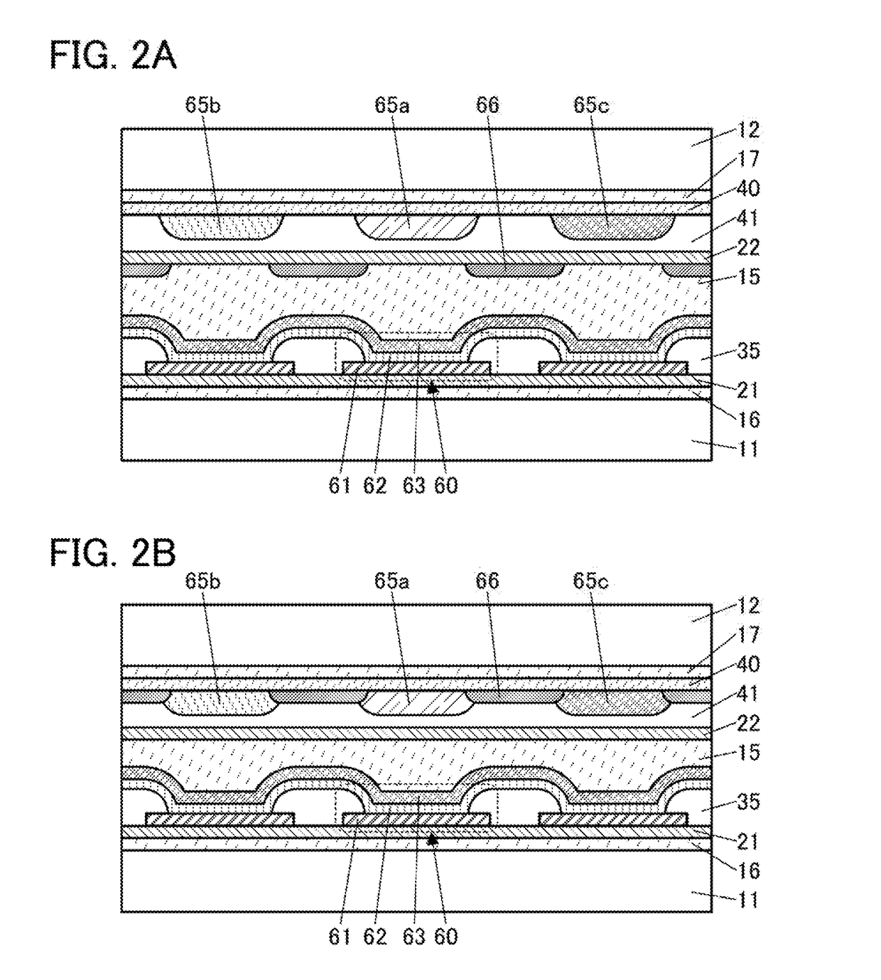
[0102]FIG. 2B shows an example of the case where the light-blocking layer 66, the coloring layer 65a, the coloring layer 65b, and the coloring layer 65c are positioned between the barrier layer 22 and the substrate 12.
[0103]In FIG. 2B, the light-blocking layer 66, the coloring layer 65a, the coloring layer 65b, and the coloring layer 65c are provided on the substrate 11 side of the insulating layer 40, and furthermore, the insulating layer 41 and the barrier layer 22 are stacked to cover these layers.
[0104]Such a structure is preferable because the barrier layer 22 can be provided in a position closer to the neutral plane of the display device 10.
[0105]In this case, the barrier layer 22 is preferably formed using a material with a higher Young's modulus than at least one or more of the coloring layers 65a to 65c, the light-blocking layer 66, the insulating layer 40, the insulating layer 41, the adhesive layer 17, and the substrate 12.
modification example 1
[0106]FIG. 3A shows an example of the case where the insulating layer 41 in FIG. 1 is not provided. FIG. 3B shows an example of the case where the insulating layer 41 in FIG. 2A is not provided. FIG. 3C shows an example of the case where the insulating layer 41 in FIG. 2B is not provided.
[0107]The display device 10 having such a structure can have a small thickness, so that stress that is applied to the barrier layer 22 by deformation such as bending of the display device 10 can be reduced. Furthermore, a step of forming the insulating layer 41 can be omitted.
PUM
Abstract
To provide a display device with high reliability. To provide a repeatedly bendable flexible display. A first substrate, a second substrate, a display element, a light-blocking layer, a first barrier layer, and an adhesive layer are included. The first substrate and the second substrate face each other. The display element, the light-blocking layer, the first barrier layer, and the adhesive layer are between the first substrate and the second substrate. The display element is between the first substrate and the adhesive layer. The light-blocking layer is between the second substrate and the adhesive layer. The first barrier layer includes a region between the light-blocking layer and the adhesive layer. The first barrier layer includes a material having a higher Young's modulus than the light-blocking layer or the adhesive layer.
Description
BACKGROUND OF THE INVENTION[0001]1. Field of the Invention[0002]One embodiment of the present invention relates to a display device. One embodiment of the present invention relates to a flexible display device.[0003]Note that one embodiment of the present invention is not limited to the above technical field. Examples of the technical field of one embodiment of the present invention disclosed in this specification and the like include a semiconductor device, a display device, a light-emitting device, a power storage device, a memory device, an electronic device, a lighting device, an input device, an input / output device, a method for driving any of them, and a method for manufacturing any of them.[0004]Note that in this specification and the like, a semiconductor device generally means a device that can function by utilizing semiconductor characteristics. A transistor, a semiconductor circuit, an arithmetic device, a memory device, and the like are each an embodiment of the semicond...
Claims
Application Information
Patent Timeline
Application Date:The date an application was filed.
Publication Date:The date a patent or application was officially published.
First Publication Date:The earliest publication date of a patent with the same application number.
Issue Date:Publication date of the patent grant document.
PCT Entry Date:The Entry date of PCT National Phase.
Estimated Expiry Date:The statutory expiry date of a patent right according to the Patent Law, and it is the longest term of protection that the patent right can achieve without the termination of the patent right due to other reasons(Term extension factor has been taken into account ).
Invalid Date:Actual expiry date is based on effective date or publication date of legal transaction data of invalid patent.

