Low cost wafer level process for packaging MEMS three dimensional devices

a three-dimensional device and low-cost technology, applied in the field of microelectromechanical device packaging, can solve the problems of the most expensive process in micromachining and the general cost-effectiveness of wafer-level packaging

Active Publication Date: 2017-08-17
RGT UNIV OF CALIFORNIA
View PDF11 Cites 4 Cited by
  • Summary
  • Abstract
  • Description
  • Claims
  • Application Information

AI Technical Summary

Benefits of technology

[0034]The packing is fabricated by including a step where heating the cap-handle wafer stack as to allow pressure buildup within the cavity causing plastic deformation of the cap wafer comprises microglassblowing a bubble in the cap wafer with a diameter of 10 mm or greater at at least 134 Torr pressure and a height of 6.8 mm or less so that removing the handle wafer to open the cavity does not break the bubble.

Problems solved by technology

It is also the most expensive process in micromachining.
However, wafer-level packaging is generally more cost effective.

Method used


Image

  • Low cost wafer level process for packaging MEMS three dimensional devices
  • Low cost wafer level process for packaging MEMS three dimensional devices
  • Low cost wafer level process for packaging MEMS three dimensional devices

Examples


Embodiment Construction

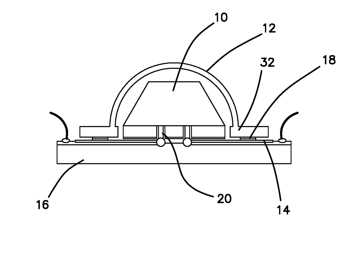
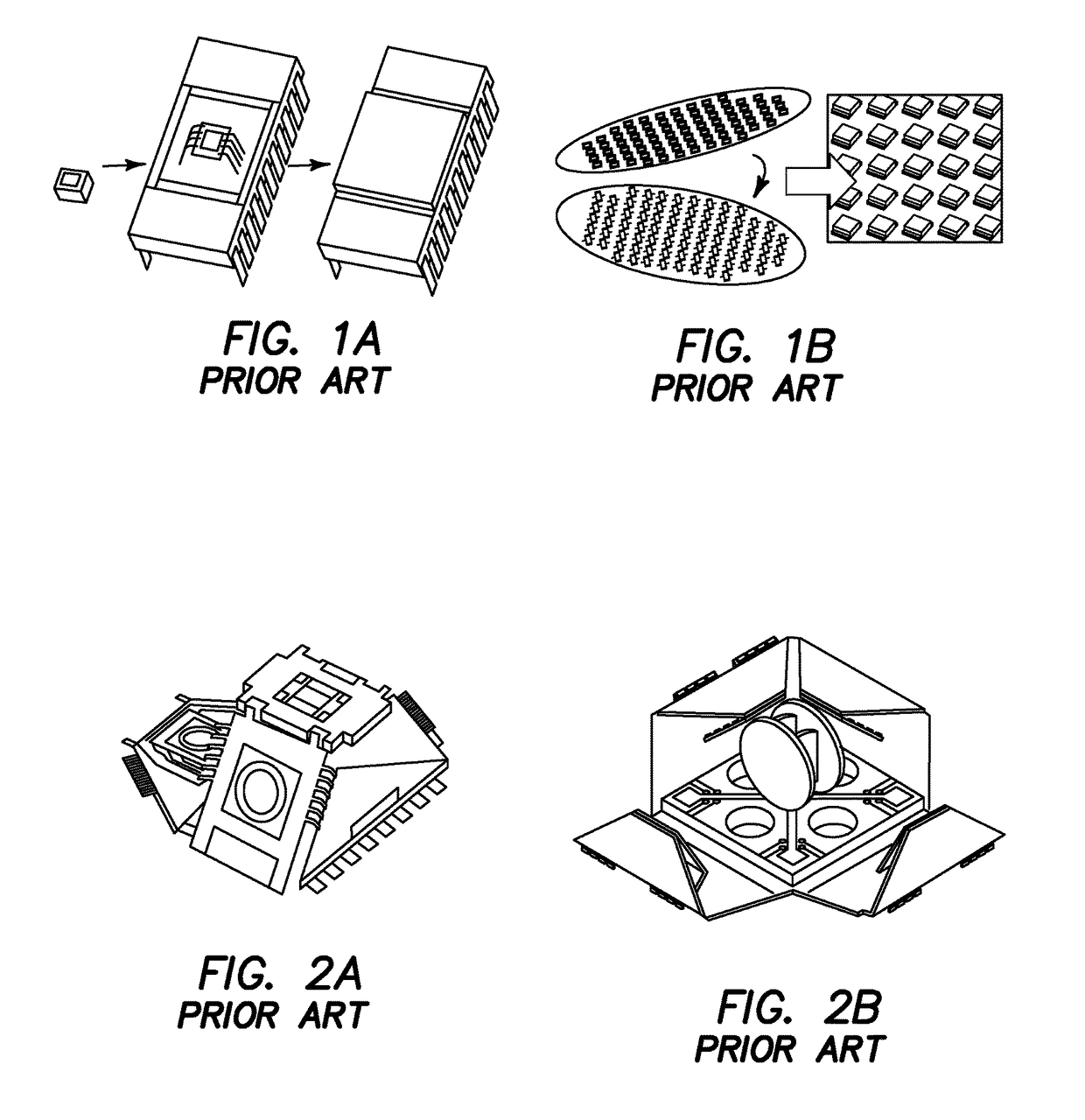
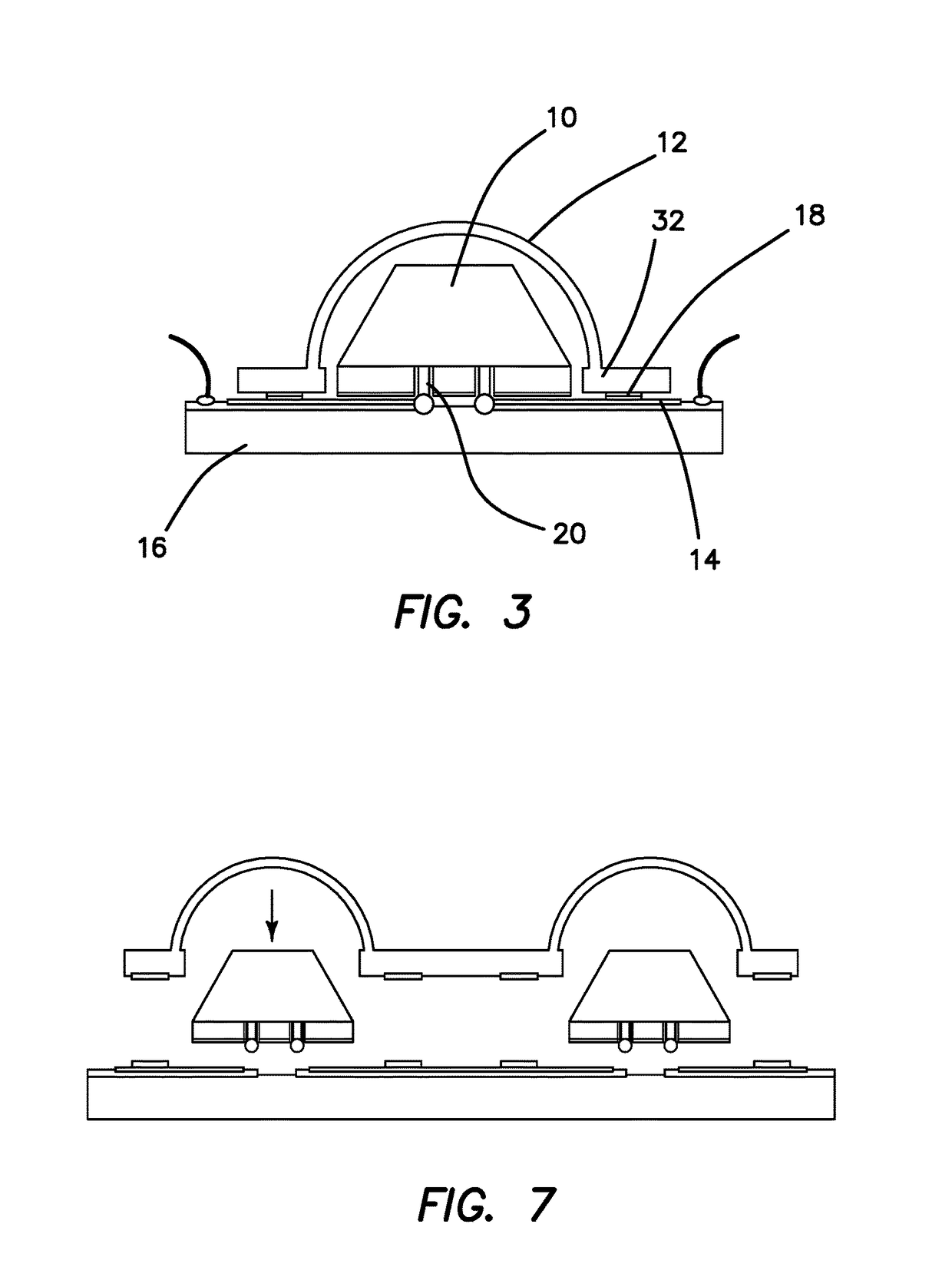
[0049]As a demonstration of using the packaging method of the illustrated embodiments of the invention, a 50 mm3 three dimensional MEMS TIMU device as shown in FIG. 2a was packaged, using the LCC standard package and a “bubble shaped” glass lid. Recent developments in the MEMS processing enable building complex-shaped three dimensional MEMS structures, including those using polymers to create three dimensional elements. One example of a three dimensional MEMS device is a folded mems inertial measurement unit (IMU), as seen in FIG. 2a. Folded IMU approach is based on wafer-level fabrication of planar structures with in-situ fabricated single-axis inertial sensors. These structures are then folded in a three dimensional shape, using co-fabricated polyimide flexible hinges. Another example is a chip-scale combinatorial atomic navigator, as seen in FIG. 2b. The device is assembled into a three dimensional configuration with Helmholtz coils and Rb vapor cell inside a three dimensional st...


PUM

PropertyMeasurementUnit
pressureaaaaaaaaaa
diameteraaaaaaaaaa
heightaaaaaaaaaa

Abstract

An apparatus and method for wafer-level hermetic packaging of MicroElectroMechanical Systems (MEMS) devices of different shapes and form factors is presented in this disclosure. The method is based on bonding a glass cap wafer with fabricated micro-glassblown “bubble-shaped” structures to the substrate glass/Si wafer. Metal traces fabricated on the substrate wafer serve to transfer signals from the sealed cavity of the bubble to the outside world. Furthermore, the method provides for chip-level packaging of MEMS three dimensional structures. The packaging method utilizes a micro glass-blowing process to create “bubbleshaped” glass lids. This new type of lids is used for vacuum packaging of three dimensional MEMS devices, using a standard commercially available type of package.

Description

RELATED APPLICATIONS[0001]This application is related to provisional patent application, entitled, A LOW-COST WAFER LEVEL PROCESS FOR PACKAGING MEMS THREE DIMENSIONAL DEVICES, Ser. No. 62 / 295991, filed on Feb. 16, 2016, under 35 USC 119, which is incorporated herein by reference.BACKGROUND[0002]Field of the Technology[0003]The invention relates to the field of semiconductor packaging, and more specifically to a package for a micro-electromechanical device. The state-of-the-art packaging technology is suitable for hermetic packaging of MEMS devices of different shapes and form factors, in particular three dimensional MEMS devices, such as a folded MEMS timing inertial measurement unit (TIMU) and MEMS atomic navigator.[0004]Description of the Prior Art[0005]Packaging for Micro-electromechanical systems (MEMS) and Integrated circuits (IC) is one of the most important manufacturing steps before bringing the product into the market. It is also the most expensive process in micromachining...

Claims


Application Information

Patent Timeline
Patent Type & Authority Applications(United States)
IPC IPC(8): B81B7/00B81C1/00
CPCB81B7/0074B81C1/00269B81C2203/019B81C2203/0118B81C2203/0127B81B2207/097B81B7/007B81C1/00634B81C3/001B81C2203/0109B81C2203/0172C03B23/0352
Inventor SHKEL, ANDREI A.EFIMOVSKAYA, ALEXANDRASENKAL, DORUK
Owner RGT UNIV OF CALIFORNIA
Why Eureka
Try Eureka