Wafer level chip scale package having continuous through hole via configuration and fabrication method thereof

a chip scale and configuration technology, applied in the field of semiconductor chip packaging, can solve the problems of interconnection failure between solder pads and the conductive material filled in through holes, difficulty in controlling the depth, and over-etching or under-etching of through holes,

Active Publication Date: 2017-09-07
POWERTECH TECHNOLOGY
View PDF8 Cites 3 Cited by
  • Summary
  • Abstract
  • Description
  • Claims
  • Application Information

AI Technical Summary

Problems solved by technology

However, it is difficult to control the depth of the through holes when performing the laser drill or the etching process, causing over-etching or under-etching of the through holes.
When the through holes are over-etched, the through holes may penetrate through the solder pads of the device chip, diffusing the etching material or etc

Method used


Image

  • Wafer level chip scale package having continuous through hole via configuration and fabrication method thereof
  • Wafer level chip scale package having continuous through hole via configuration and fabrication method thereof
  • Wafer level chip scale package having continuous through hole via configuration and fabrication method thereof

Examples


Embodiment Construction

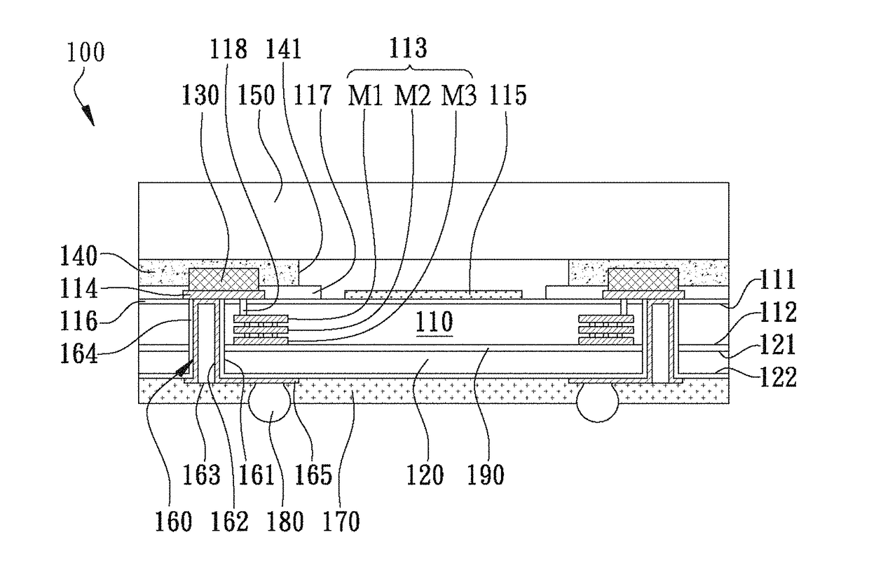
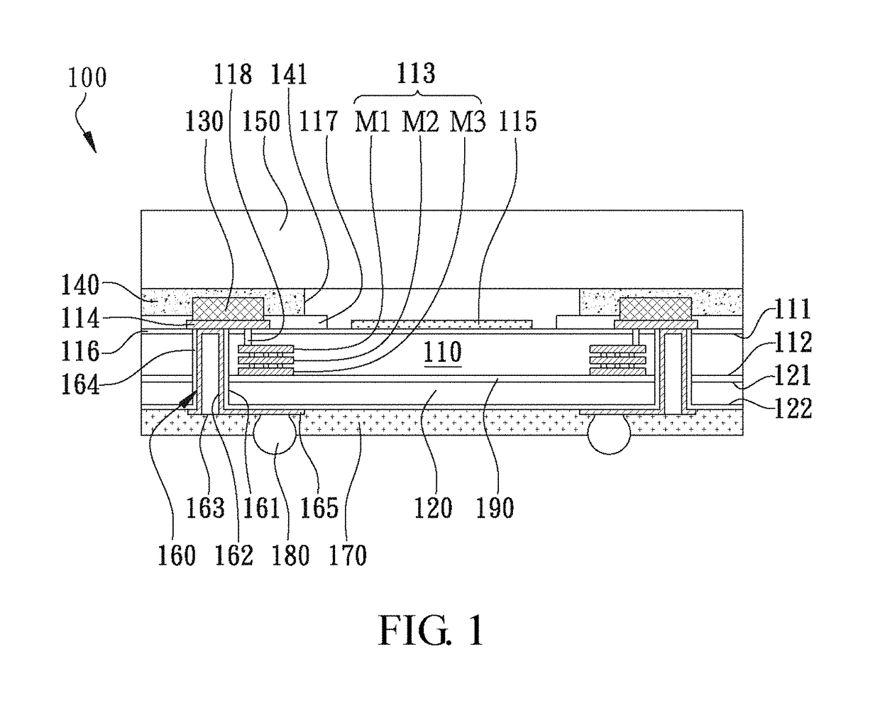
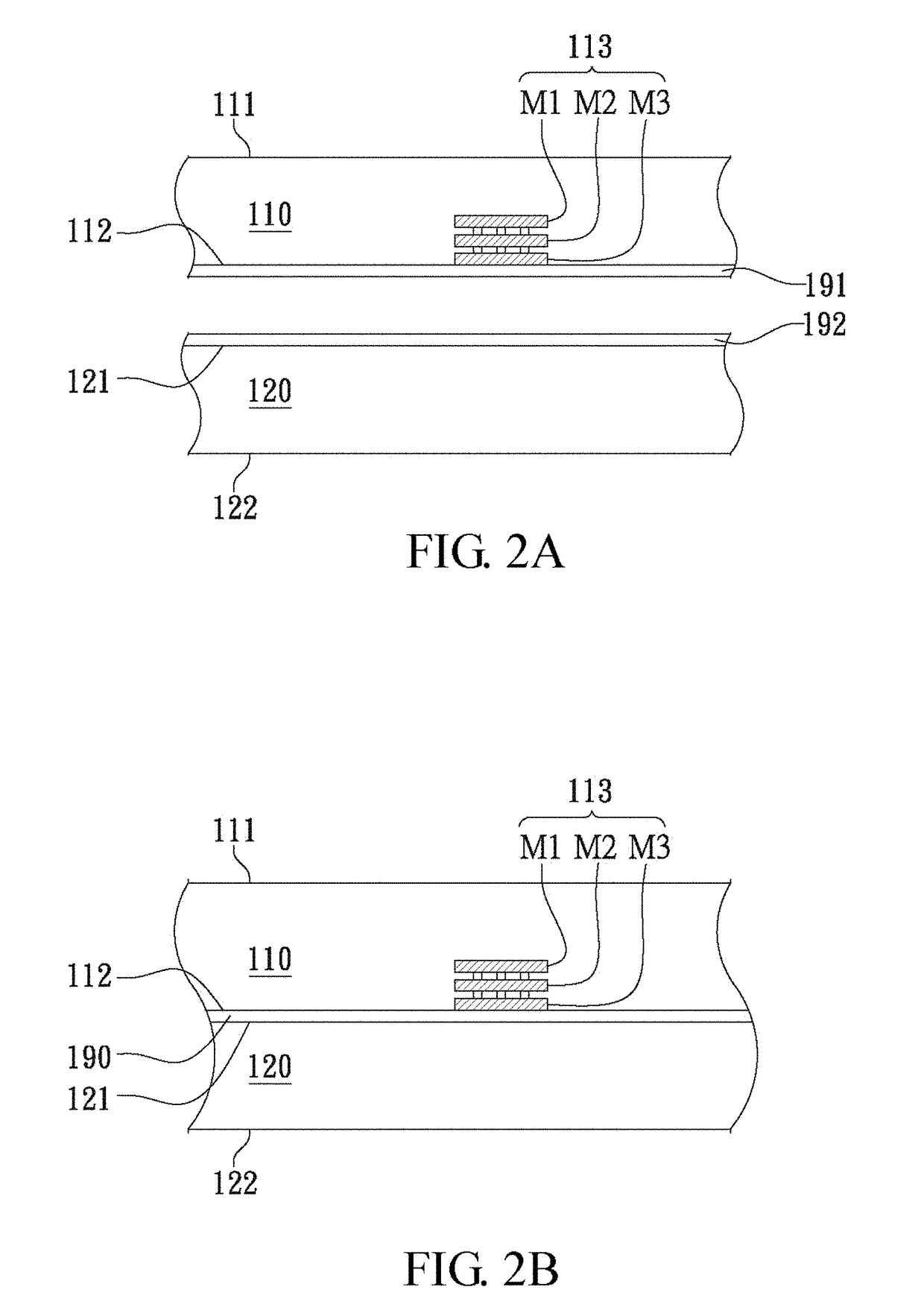
[0013]With reference to the attached drawings, the present invention is described by means of the embodiment(s) below where the attached drawings are simplified for illustration purposes only to illustrate the structures or methods of the present invention by describing the relationships between the components and assembly in the present invention. Therefore, the components shown in the figures are not expressed with the actual numbers, actual shapes, actual dimensions, nor with the actual ratio. Some of the dimensions or dimension ratios have been enlarged or simplified to provide a better illustration. The actual numbers, actual shapes, or actual dimension ratios can be selectively designed and disposed and the detail component layouts may be more complicated.

[0014]According to a first embodiment of the present invention, a wafer level chip scale package (WLCSP) 100 having continuous through hole via (THV) configuration is illustrated in FIG. 1 for a cross-sectional view. The WLCS...


PUM


Abstract

A wafer level chip scale package (WLCSP) has a device chip, a carrier chip, an offset pad, a conductive spacing bump and a through hole via (THV). The device chip is attached to the carrier chip. The offset pad is disposed on a first surface of the device chip. The conductive spacing bump is formed on the offset pad. The through hole via includes a through hole and a hole metal layer. The through hole penetrates through the carrier chip and the device chip, and the hole metal layer is formed in the through hole and in contact with the offset pad.

Description

BACKGROUND OF THE INVENTION[0001]1. Field of the Invention[0002]The present invention relates to packaging semiconductor chips, and more particularly to a wafer level chip scale package (WLCSP) having continuous through hole vias (THVs) and a fabrication method thereof.[0003]2. Description of the Prior Art[0004]A wafer level chip scale package (WLCSP) is different from a conventional semiconductor package. The integrated circuits of the WLCSP are tested and packaged in the wafer stage before dicing the WLCSP. The size of the WLCSP is not greater than 1.44 times of the size of the chips. A WLCSP usually has double-sided longitudinal electrical interconnections for connecting terminals to the bottom of the chip to reduce the size of the substrate or omit the substrate. A conventional double-sided longitudinal electrical interconnection may be a through hole via (THV) or a chip side redistribution layer (RDL).[0005]In the packaging process of a conventional WLCSP using through hole via...

Claims


Application Information

Patent Timeline
IPC IPC(8): H01L23/31H01L23/00H01L27/146H01L21/56H01L21/768H01L23/48H01L23/498
CPCH01L23/3114H01L2224/13155H01L24/06H01L24/13H01L23/562H01L23/49827H01L23/3121H01L24/83H01L24/03H01L24/11H01L21/56H01L21/76898H01L24/32H01L27/14618H01L27/14627H01L27/14636H01L27/14632H01L2224/0401H01L2224/11462H01L2224/1134H01L2224/0237H01L2924/15311H01L2224/32225H01L2224/73253H01L2224/13027H01L2224/13016H01L2224/05124H01L2224/05147H01L2924/0132H01L2224/13144H01L2224/13139H01L2224/13147H01L23/481H01L21/561H01L23/3107H01L23/3128H01L23/49816H01L23/49838
Inventor FANG, LI-CHIHCHANG, CHIA-CHANGHSU, HUNG-HSINCHANG, WEN-HSIUNGCHUNG, KEE-WEILIEN, CHIA-WEN
Owner POWERTECH TECHNOLOGY
Why Eureka
Try Eureka