Multi-level metalization on a ceramic substrate

Active Publication Date: 2017-10-05
CERAMTEC
View PDF4 Cites 3 Cited by
  • Summary
  • Abstract
  • Description
  • Claims
  • Application Information

AI Technical Summary

Benefits of technology

[0007]The object of the invention is to improve a method according to the preamble of claim 1, so that with simple means metalizations for high power areas and metalizations for low power areas can be printed

Problems solved by technology

These connections age and incline to failure, which results in breakdown of the entire power module.
To date, the production of such a multi-stage substrate

Method used


Image

  • Multi-level metalization on a ceramic substrate
  • Multi-level metalization on a ceramic substrate

Examples


Example

EXAMPLE

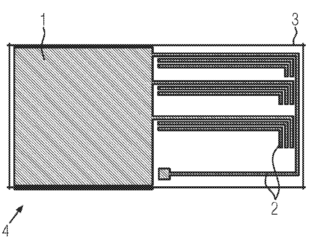
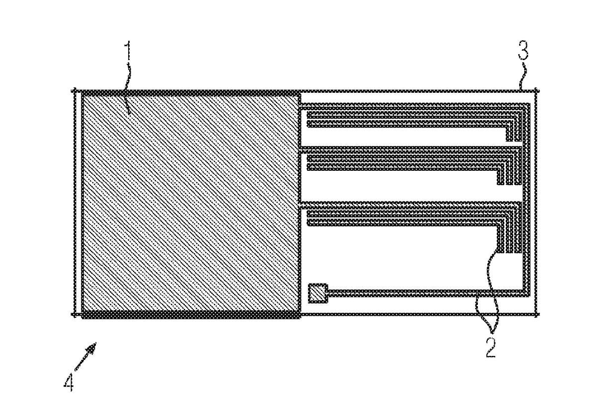
[0028]First of all, the entire electrical layout consisting of a high power area and a low power area is printed as metalization 50 μm high with a copper-based paste having a glass portion of 6% on a lasered ceramic substrate consisting of AlN having a thickness of 0.63 mm. Laser treatment of the ceramic substrate ensures, so that later a separation by severing along the break line is possible. Then only the high power area or the metalization thereof, upon which the power component is later soldered, is brought to a 350 μm metalization thickness by further multiple screen or stencil printing processes using a copper-based paste without glass component. Thereafter the metalized component is annealed at 910° C. for 8 min under N2.

[0029]The high power area of the metalized and annealed ceramic substrate by itself is then in this example 310 μm high. The metalization of the low power area is 40 μm high. The high power area and / or copper thereof is then mechanically leveled by a ...


PUM

PropertyMeasurementUnit
Temperatureaaaaaaaaaa
Lengthaaaaaaaaaa
Lengthaaaaaaaaaa

Abstract

A method for producing a copper multi-level metallization on a ceramic substrate consisting of AlN or Al2O3. High power regions with metallization having a high current-carrying capacity and low power regions with metallic coatings having a low current-carrying capacity are created on one and the same ceramic substrate. The metallization is printed multiple times in the high power range.

Description

CROSS REFERENCE TO RELATED APPLICATIONS[0001]This application is a continuation of U.S. application Ser. No. 14 / 763,694 filed Jul. 28, 2015, pending, which is a §371 of International Application No. PCT / EP2014 / 052177 filed Feb. 5, 2014, and claims priority from German Patent Application No. 10 2013 202 008.2 filed Feb. 7, 2013, each of which is incorporated herein by reference in its entirety for all purposes.FIELD OF THE INVENTION[0002]The invention relates to a method for producing a copper multi-level metalization on a ceramic substrate composed of AlN or Al2O3, whereby high power areas with metalization having higher current-carrying capacity and low power areas with metalization having lower current-carrying capacity are created on one and the same ceramic substrate.BACKGROUND OF THE INVENTION[0003]Metalized ceramic substrates, also referred to as printed circuit boards, having a thick copper layer (typically 200 to 300 μm) are required for power electronic applications, to ens...

Claims


Application Information

Patent Timeline
IPC IPC(8): H05K3/12H01L21/48H05K1/03C22F1/08H01L23/498H05K3/22
CPCH01L23/49844H01L21/4867H01L2924/0002H05K1/0306H05K3/1216Y10T428/24355C22F1/08H05K3/22H01L2924/00
Inventor ADLER, SIGURDDILSCH, ROLANDTHIMM, ALFRED
Owner CERAMTEC
Why Eureka
Try Eureka