

Semiconductor device
a technology of semiconductors and devices, applied in semiconductor/solid-state device details, amplifiers with semiconductor devices/discharge tubes, amplifiers wit coupling networks, etc., can solve the problem of difficulty in reducing chip cost by chip area, and achieve the effect of reducing chip cost and chip area
- Summary
- Abstract
- Description
- Claims
- Application Information
AI Technical Summary
Benefits of technology
Problems solved by technology
Method used
Image

Examples
first embodiment
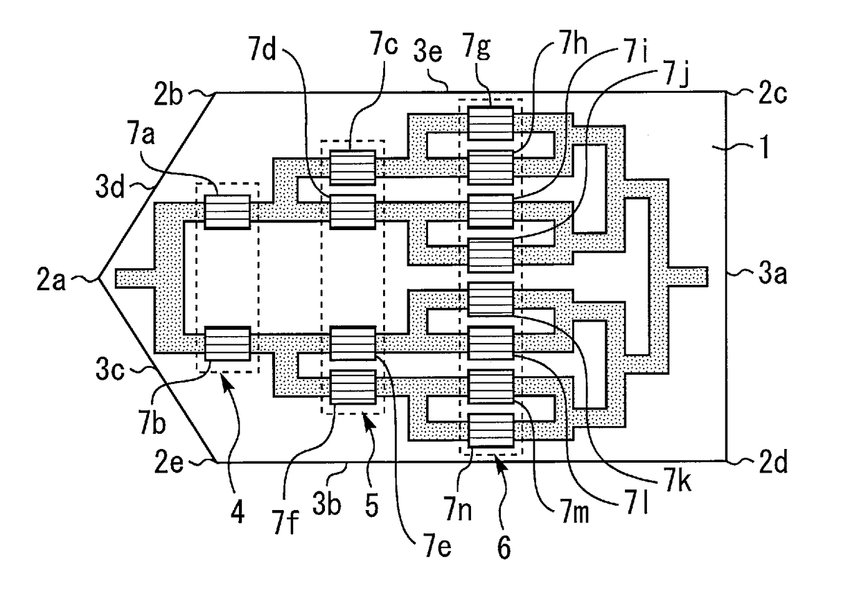
[0016]FIG. 1 is a plan view of a semiconductor device according to a first embodiment of the present invention. The contour of the semiconductor substrate 1 is a pentagon having five vertices 2a to 2e and five sides 3a to 3e. The side 3a is opposed to the vertex 2a. The vertex 2a is placed on a perpendicular to the side 3a passing through the middle point of the side 3a. The sides 3b and 3e are parallel to each other and equal in length to each other. The sides 3c and 3d are equal in length to each other.
[0017]An MMIC of a three-stage configuration is formed on the semiconductor substrate 1. An amplifier 5 in the second stage amplifies outputs from an amplifier 4 in the first stage, and an amplifier 6 in the final stage amplifies outputs from the amplifier 5 in the second stage. The amplifier 4 in the first stage has two FETs 7a and 7b. The amplifier 5 in the second stage has four FETs 7c to 7f. The amplifier 6 in the final stage has eight FETs 7g to 7n. Thus, the number of transist...
second embodiment
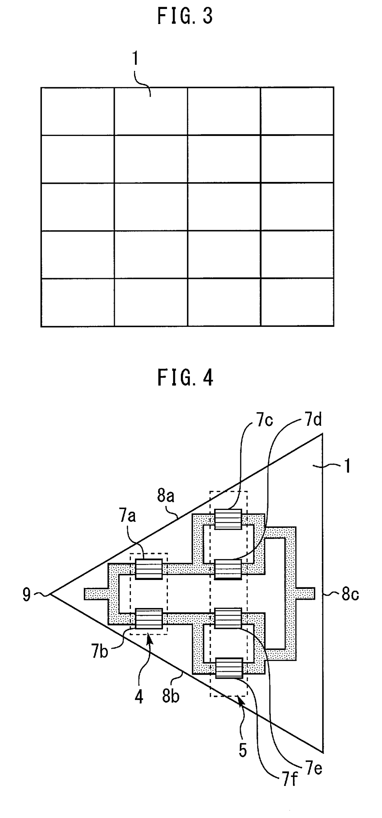
[0022]FIG. 4 is a plan view showing a semiconductor device according to a second embodiment of the present invention. In the second embodiment, the contour of the semiconductor substrate 1 is an isosceles triangle having two first and second equal sides 8a and 8b equal in length to each other, and a bottom side 8c. The front-stage amplifier 4 is formed relatively near a vertex 9 shared by the first and second equal sides 8a and 8b of the semiconductor substrate 1, while the rear-stage amplifier 5 is formed relatively near the bottom side 8c of the semiconductor substrate 1. Empty spaces on the front stage side can thereby be reduced in comparison with the case of the conventional rectangular semiconductor substrate. The chip area can thus be reduced to reduce the chip cost.
[0023]FIG. 5 is a plan view showing a state where semiconductor substrates in isosceles triangle form are arranged on a wafer. The semiconductor substrates 1 are alternately arranged as illustrated and can thus be...
third embodiment
[0024]FIG. 6 is a plan view showing a semiconductor device according to a third embodiment of the present invention. In the third embodiment, the contour of the semiconductor substrate 1 is an isosceles trapezoid having an upper base 10a and a lower base 10b parallel to the upper base 10a and longer than the upper base 10a. The front-stage amplifier 4 is formed relatively near the upper base 10a of the semiconductor substrate 1, while the rear-stage amplifier 5 is formed relatively near the lower base 10b of the semiconductor substrate 1. Empty spaces on the front stage side can thereby be reduced in comparison with the case of the conventional rectangular semiconductor substrate. The chip area can thus be reduced to reduce the chip cost.
[0025]FIG. 7 is a plan view showing a state where semiconductor substrates in isosceles trapezoid form are arranged on a wafer. The semiconductor substrates 1 are alternately arranged as illustrated and can thus be laid on the wafer with no margin. ...
PUM
 Abstract
Description
Claims
Application Information