Deposition of metal borides and silicides

a metal boride and metal boride technology, applied in chemical vapor deposition coatings, coatings, metallic material coating processes, etc., can solve the problems of low conformality, insufficient thin film coverage, and high substrate temperature relative to thermal budgets

Active Publication Date: 2017-10-26
ASM IP HLDG BV
View PDF25 Cites 306 Cited by
  • Summary
  • Abstract
  • Description
  • Claims
  • Application Information

AI Technical Summary

Problems solved by technology

In order to thermally activate some of the gaseous source chemicals, the CVD methods tend to take place at temperatures as high as 1200° C. The high substrate temperatures relative to thermal budgets may be problematic, especially for state-of-the-art semiconductor fabrication processes such as metallization.
However, line-of-sight deposition results in insufficient thin film coverage in certain areas where complex substrate contours are involved.
Also, line-of-sight deposition results in low-volatility precursors depositing on the first solid surface encountered, leading to low-conformality coverage.
However, no known ALD solution exists to deposit metal boride or metal silicide films at low temperatures.

Method used


Image

  • Deposition of metal borides and silicides
  • Deposition of metal borides and silicides
  • Deposition of metal borides and silicides

Examples


Embodiment Construction

[0014]Although certain embodiments and examples are disclosed below, it will be understood by those in the art that the invention extends beyond the specifically disclosed embodiments and / or uses of the invention and obvious modifications and equivalents thereof. Thus, it is intended that the scope of the invention disclosed should not be limited by the particular disclosed embodiments described below.

[0015]Metal boride and metal silicide films demonstrate potential use in a myriad of applications due to their characteristics. For example, these metal films have a low work function and low resistivity, which make such films ideal for n-metal gate or gate fill applications. Also, the high chemical resistance of metal borides and metal silicides makes them applicable for use in patterning layers and hard masks. Furthermore, the high work function and low resistivity of metal films provide for applicability in p-metal stack, gate fill, and MIMCAP electrodes (SoC).

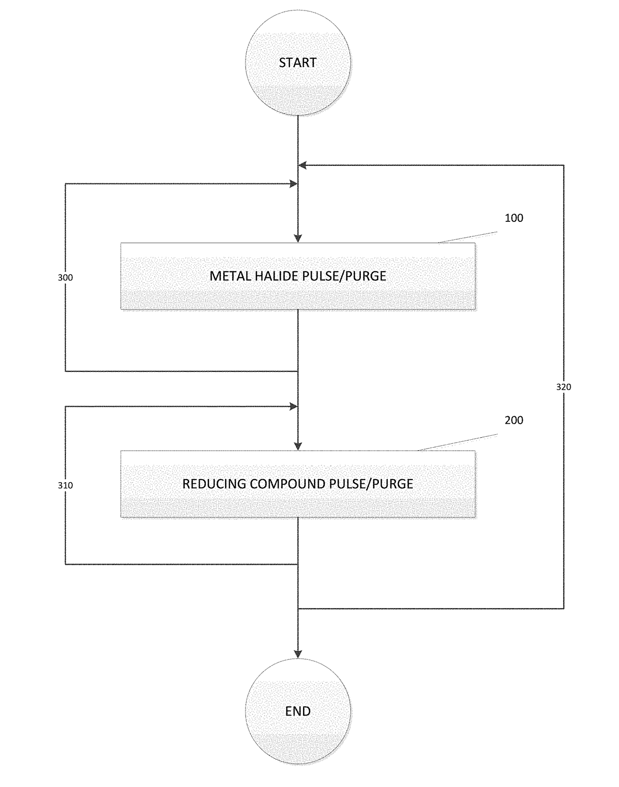
[0016]FIG. 1 illustrat...


PUM

PropertyMeasurementUnit
temperatureaaaaaaaaaa
pressureaaaaaaaaaa

Abstract

A method for depositing a metal film onto a substrate is disclosed. In particular, the method comprises pulsing a metal halide precursor onto the substrate and pulsing a reducing precursor onto the substrate. A reaction between the metal halide precursor and the reducing precursor forms a metal film. Specifically, the method discloses forming a metal boride or a metal silicide film.

Description

CROSS-REFERENCE TO RELATED APPLICATION[0001]This application is related to U.S. Non-Provisional patent application Ser. No. 15 / 135,224, concurrently filed and entitled “DEPOSITION OF METAL BORIDES” and U.S. Non-Provisional application Ser. No. ______, concurrently filed and entitled “DEPOSITION OF METAL BORIDES,” the disclosures of which are hereby incorporated by reference in their entireties.FIELD OF INVENTION[0002]The present disclosure generally relates to processes for manufacturing electronic devices. More particularly, the disclosure relates to forming metal gates through atomic layer deposition (ALD). Specifically, the disclosure relates to forming metal silicides and metal borides.BACKGROUND OF THE DISCLOSURE[0003]Metal boride and metal silicide films have been formed using various chemical vapor deposition (CVD) methods. In the CVD methods, gaseous source chemicals are introduced into a reaction space at the same time, resulting in a deposition of a metal film on the subst...

Claims


Application Information

Patent Timeline
Patent Type & Authority Applications(United States)
IPC IPC(8): C23C16/38C23C16/455C23C16/42
CPCC23C16/38C23C16/42C23C16/45525C23C16/45553H01L21/02104H01L21/28194H01L21/28061H01L21/28556H01L21/02205H01L21/02041H01L21/67248
Inventor RAISANEN, PETRISHERO, ERICHAUKKA, SUVIMILLIGAN, ROBERT BRENNANGIVENS, MICHAEL EUGENE
Owner ASM IP HLDG BV
Why Eureka
Try Eureka