Display device, display module, electronic device, and driving method

Active Publication Date: 2017-12-07
SEMICON ENERGY LAB CO LTD
View PDF3 Cites 14 Cited by
  • Summary
  • Abstract
  • Description
  • Claims
  • Application Information

AI Technical Summary

Benefits of technology

[0024]One embodiment of the present invention can provide a display device with a novel structure. Another object of one embodiment of the present invention can

Problems solved by technology

In hold-type driving, a moving image blur is generated in a display region owing to an active-matrix display; thus, there is a problem in that the edge of a displayed moving image or the like becomes unclear, for examp

Method used


Image

  • Display device, display module, electronic device, and driving method
  • Display device, display module, electronic device, and driving method
  • Display device, display module, electronic device, and driving method

Examples


embodiment 1

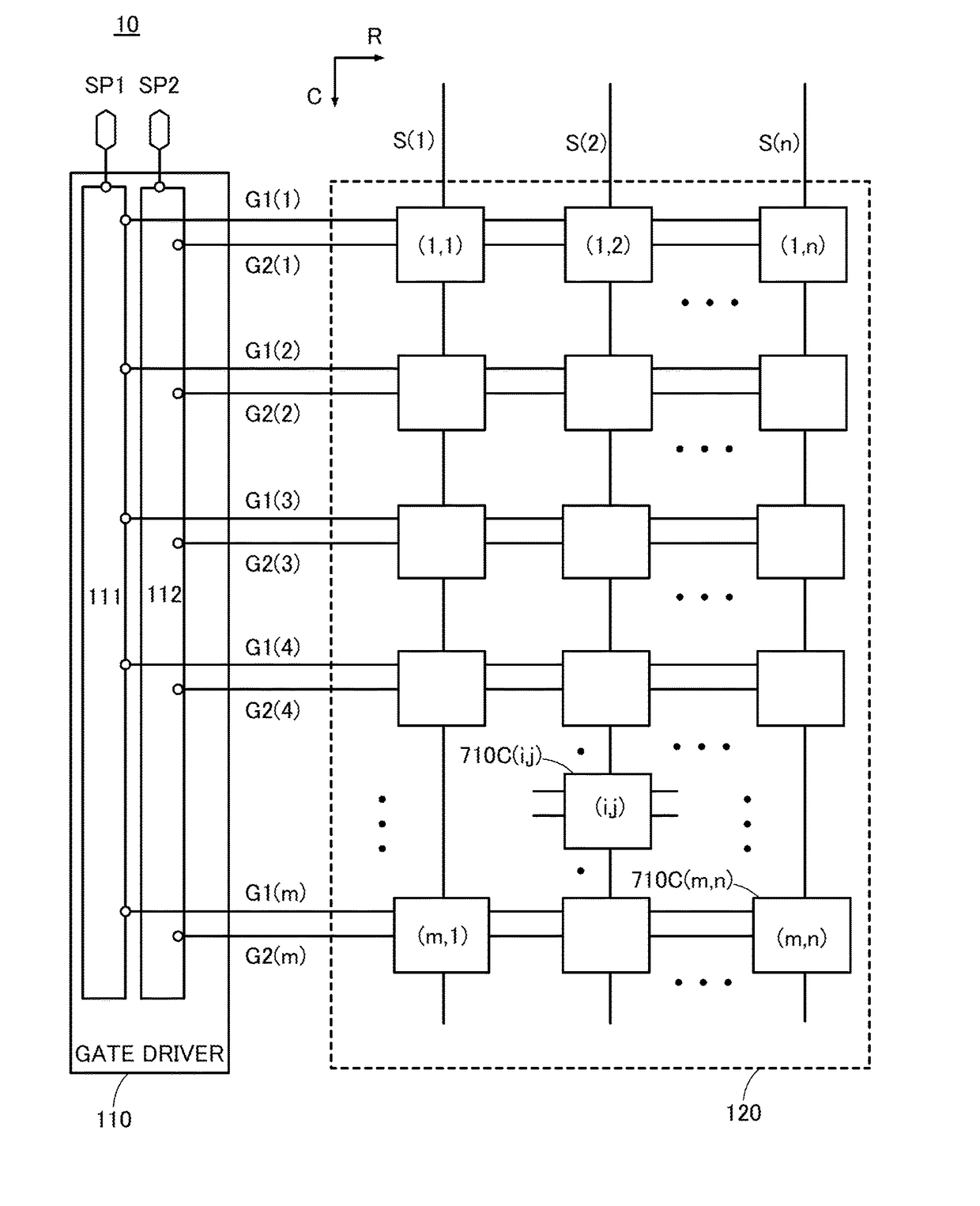
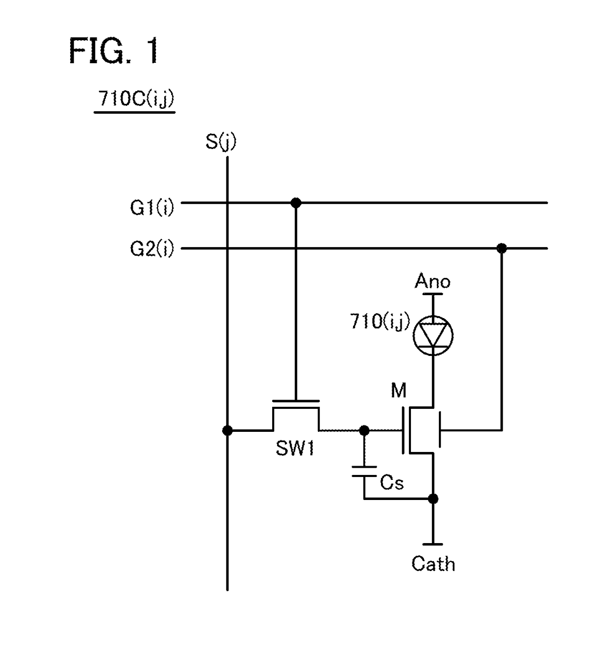
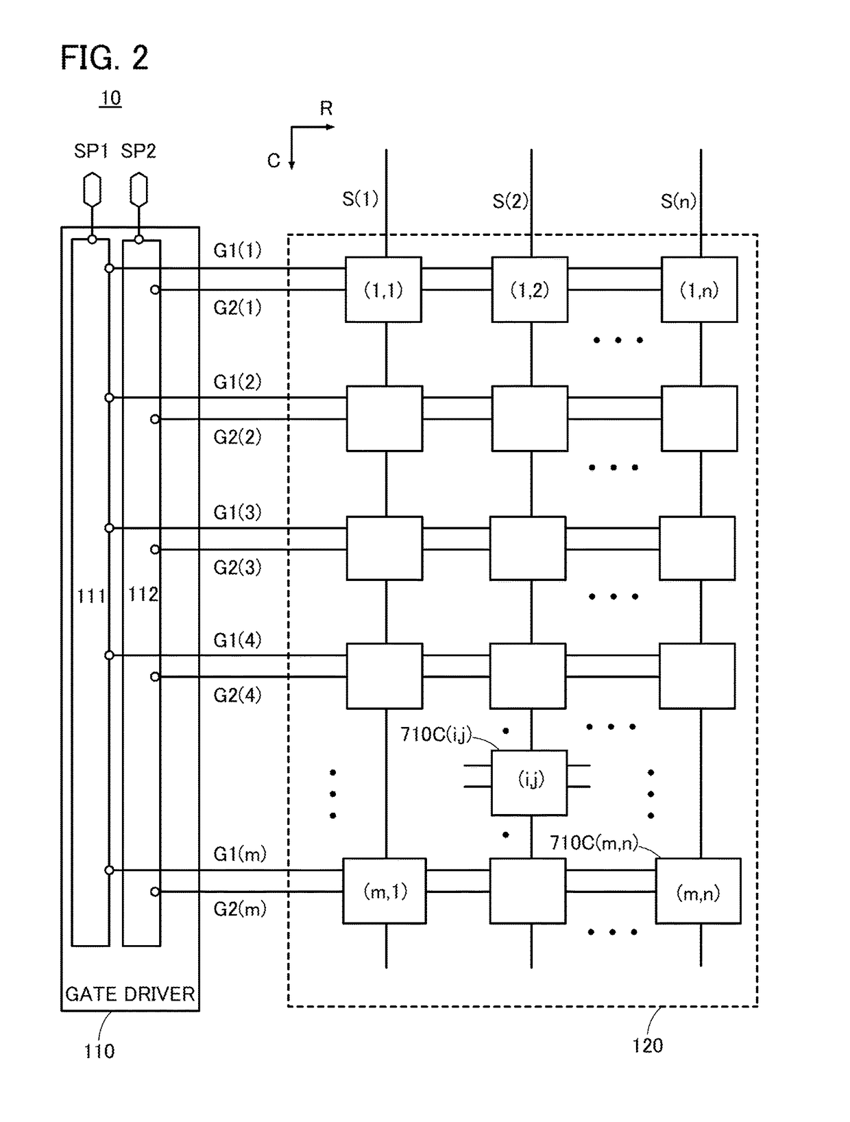
[0061]In this embodiment, a display device that has a function of controlling display by supply of a signal from a scan line electrically connected to a back gate of a transistor included in a pixel circuit is described with reference to FIG. 1, FIG. 2, FIGS. 3A and 3B, FIG. 4, FIGS. 5A and 5B, and FIGS. 6A to 6D.

[0062]FIG. 1 illustrates the structure of a pixel circuit 710C(i,j). FIG. 2 is a block diagram illustrating the structure of a display device 10. One pixel circuit in a display portion 120 of the display device 10 in FIG. 2 is described as the pixel circuit 710C(i,j). The display portion 120 includes m (row direction)×n (column direction) pixel circuits in a matrix, where m is an integer greater than or equal to 1 and n is an integer greater than or equal to 1. Note that i is an integer greater than or equal to 1 and less than or equal to m, and j is an integer greater than or equal to 1 and less than or equal to n.

[0063]The pixel circuit 710C(i,j) includes a light-emitting...

embodiment 2

[0106]In this embodiment, an IC chip, an electronic component, an electronic device, and the like are described as examples of a semiconductor device.

[0107]FIG. 7A is a flow chart showing an example of a method for manufacturing an electronic component. The electronic component is also referred to as a semiconductor package or an IC package. This electronic component has a plurality of standards and names depending on a terminal extraction direction and a terminal shape. Examples of the electronic component are described in this embodiment.

[0108]A semiconductor device including a transistor is completed by integrating detachable components on a printed circuit board through an assembly process (post-process). The post-process can be finished through steps in FIG. 7A.

[0109]Specifically, after an element substrate obtained in a wafer process is completed (step ST61), a rear surface of the substrate is ground. The substrate is thinned in this step to reduce warpage or the like of the s...

embodiment 3

[0117]In this embodiment, more specific structure examples of the display panel described in any of the above embodiments are described with reference to FIGS. 8A to 8C, FIGS. 9A to 9C, FIGS. 10A and 10B, FIGS. 11A and 11B, and FIGS. 12A and 12B. Note that in this embodiment, a display panel including a liquid crystal element and a display panel including a light-emitting element are described as examples of the display panel.

[0118]FIGS. 8A to 8C are top views each illustrating a structure example of the display panel.

[0119]In FIG. 8A, a sealant 4005 is provided to surround a pixel portion 402 provided over a first substrate 4001, and the pixel portion 402 is sealed by the sealant 4005 and a second substrate 4006. In FIG. 8A, a signal line driver circuit 400 and a scan line driver circuit 401 are each formed using a single crystal semiconductor or a polycrystalline semiconductor over another substrate in a region different from a region surrounded by the sealant 4005 over the first ...


PUM


Abstract

Control of a light emission period of a light-emitting element results in higher visibility. A display device includes a signal line, a first scan line, a second scan line, and a pixel circuit. The pixel circuit includes a light-emitting element, a first transistor, and a second transistor. The second transistor includes a back gate. The second scan line is electrically connected to the back gate. The second scan line has a function of controlling the threshold voltage of the second transistor and a function of controlling the light emission period of the light-emitting element.

Description

BACKGROUND OF THE INVENTION1. Field of the Invention[0001]One embodiment of the present invention relates to a display device, a display module, and an electronic device.[0002]Note that one embodiment of the present invention is not limited to the above technical field. The technical field of one embodiment of the invention disclosed in this specification and the like relates to an object, a method, or a manufacturing method. The present invention relates to a process, a machine, manufacture, or a composition of matter. In particular, one embodiment of the present invention relates to a semiconductor device, a display device, a light-emitting device, a power storage device, a storage device, a driving method thereof, or a manufacturing method thereof.2. Description of the Related Art[0003]Mobile devices such as smartphones and tablets have become increasingly popular. In addition, novel devices such as head-mounted displays and digitized car-mounted display devices have been used, a...

Claims


Application Information

Patent Timeline
IPC IPC(8): G09G3/3233G09G3/3266H01L29/786H01L27/12G09G3/3258G09G3/36G02F1/1368H01L27/32
CPCG09G3/3233H01L27/1225H01L29/7869H01L29/78648G09G3/3258G09G3/3266G09G2320/0271H01L27/3262G02F1/1368G09G2300/0426G09G2320/0626G09G2310/08G09G3/3677G09G2300/0819G09G2300/0842G09G2300/0861G09G2310/067G09G2320/045G09G2330/021G09G2230/00G09G2300/08H10K59/1213
Inventor MIYAKE, HIROYUKI
Owner SEMICON ENERGY LAB CO LTD
Why Eureka
Try Eureka