Method for fabricating a substrate-guided optical device

a substrate-guided optical and optical element technology, applied in the field of substrate-guided optical devices, can solve the problems of inconvenient operation, large size of conventional optical modules etc., and achieve the effect of convenient exploitation of compact light-guide optical elements, large emb values, and easy incorporation

Inactive Publication Date: 2017-12-21
LUMUS LTD
View PDF3 Cites 51 Cited by
  • Summary
  • Abstract
  • Description
  • Claims
  • Application Information

AI Technical Summary

Benefits of technology

[0006]The present invention facilitates the exploitation of very compact light-guide optical element (LOE) for, amongst other applications, HMDs. The invention allows relatively wide FOVs together with relatively large EMB values. The resulting optical system offers a large, high-quality image, which also accommodates large movements of the eye. The optical system offered by the present invention is particularly advantageous because it is substantially more compact than state-of-the-art implementations and yet it can be readily incorporated, even into optical systems having specialized configurations.

Problems solved by technology

As the desired field-of-view (FOV) of the system increases, however, such a conventional optical module becomes larger, heavier and bulkier, and therefore, even for a moderate performance device, is impractical.
This is a major drawback for all kinds of displays and especially in head-mounted applications, wherein the system should necessarily be as light and as compact as possible.
The strive for compactness has led to several different complex optical solutions, all of which, on the one hand, are still not sufficiently compact for most practical applications and, on the other hand, suffer major drawbacks in terms of manufacturability.
Furthermore, the eye-motion-box (EMB) of the optical viewing angles resulting from these designs is usually very small—typically less than 8 mm Hence, the performance of the optical system is very sensitive, even for small movements of the optical system relative to the eye of the viewer, and does not allow sufficient pupil motion for comfortable reading of text from such displays.

Method used


Image

  • Method for fabricating a substrate-guided optical device
  • Method for fabricating a substrate-guided optical device
  • Method for fabricating a substrate-guided optical device

Examples


Embodiment Construction

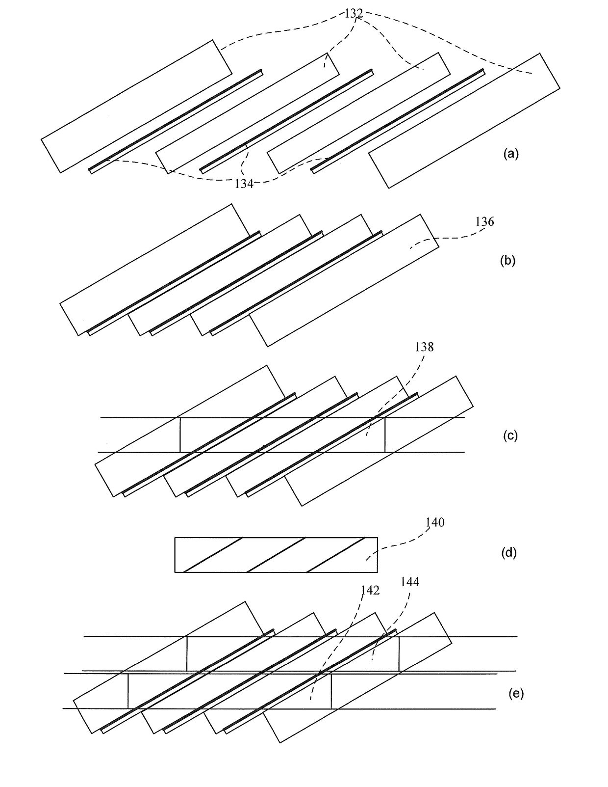
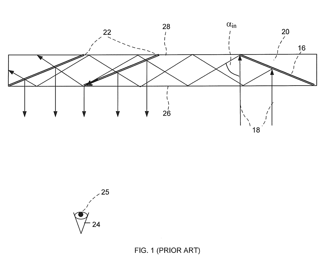
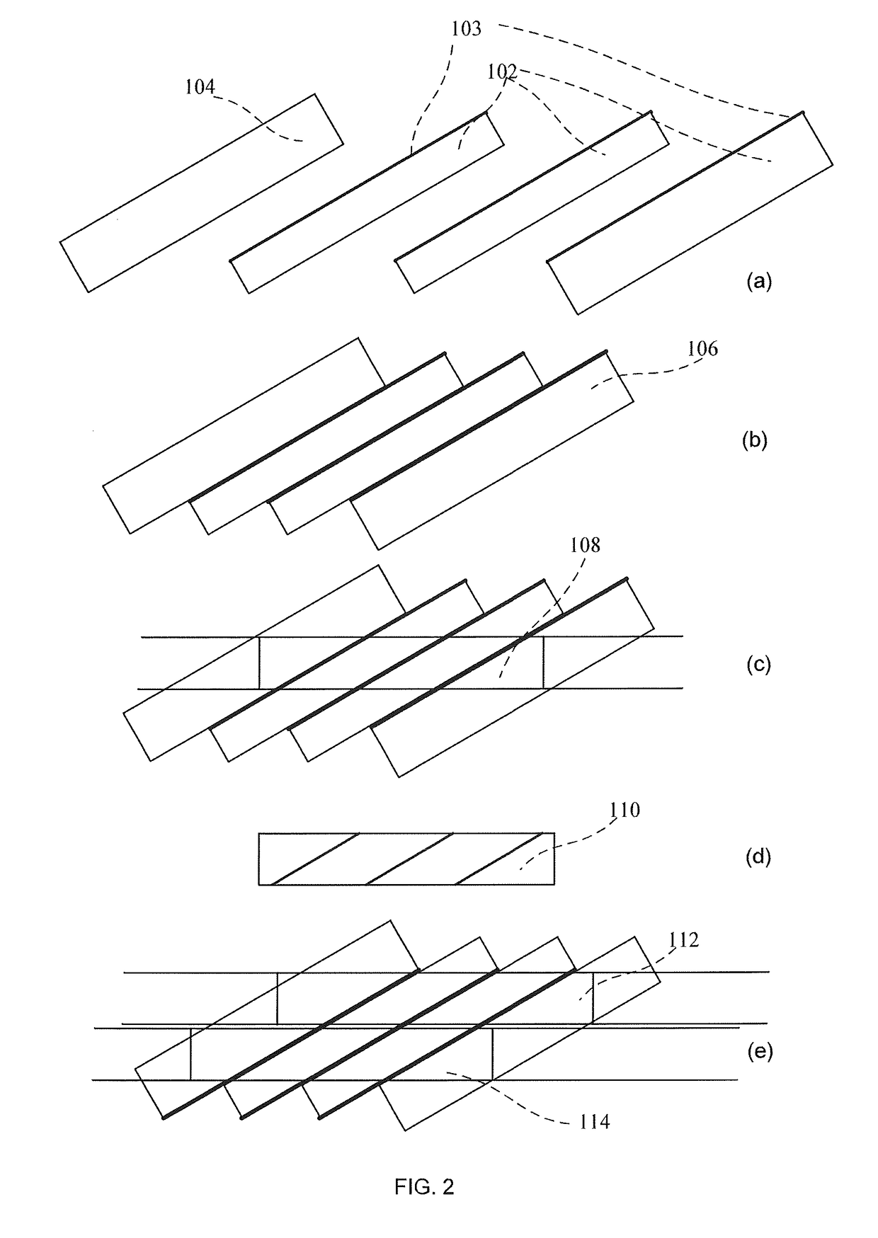
[0020]FIG. 1 illustrates a sectional view of a prior art substrate 20 and associated components (hereinafter also “an LOE”), utilizable in the present invention. An optical means, e.g., a reflecting surface 16, is illuminated by a collimated display light waves 18, emanating from a light source (not shown). The reflecting surface 16 reflects incident light waves from the source, such that the light waves are trapped inside a planar substrate 20 of the LOE, by total internal reflection. After several reflections off the major lower and upper surfaces 26, 28 of the substrate 20, the trapped light waves reach an array of selective reflecting surfaces 22, which couple the light out of the substrate into an eye 24, having a pupil 25, of a viewer. Herein, the input surface of the LOE will be regarded as the surface through which the input light waves enter the LOE and the output surface of the LOE will be regarded as the surface through which the trapped light waves exit the LOE. In the c...


PUM


Abstract

A method is described for fabricating an optical device that includes a light waves-transmitting substrate having at least two major surfaces and edges and a plurality of partially reflecting surfaces carried by the substrate, wherein the partially reflecting surfaces are parallel to each other and not parallel to any of the edges of the substrate. The method includes providing at least one transparent flat plate and plates having partially reflecting surfaces and optically attaching together the flat plates so as to create a stacked, staggered form. From the stacked, staggered form, at least one segment is sliced off by cutting across several plates and the segment is ground and polished to produce the light waves-transmitting substrate. The plates are optically attached to each other by an optically adhesive-free process.

Description

FIELD OF THE INVENTION[0001]The present invention relates to substrate-guided optical devices, and particularly to devices which include a plurality of reflecting surfaces carried by a common light-transmissive substrate, also referred to as a light-guide element.[0002]The invention can be implemented to advantage in a large number of imaging applications, such as portable DVDs, cellular phone, mobile TV receiver, video games, portable media players or any other mobile display devices.BACKGROUND OF THE INVENTION[0003]An important application for compact optical elements is in head-mounted displays (HMDs), wherein an optical module serves both as an imaging lens and a combiner, in which a two-dimensional image source is imaged to infinity and reflected into the eye of an observer. The display source can be directly obtained from either a spatial light modulator (SLM) such as a cathode ray tube (CRT), a liquid crystal display (LCD), an organic light emitting diode array (OLED), a scan...

Claims


Application Information

Patent Timeline
Patent Type & Authority Applications(United States)
IPC IPC(8): F21V8/00G02B27/01
CPCG02B6/0065G02B2027/0123G02B6/0076G02B27/0172G02B6/00G02B2027/0125G02B6/008G02B6/0008
Inventor OFIR, YUVALFRIEDMANN, EDGARAMITAI, YAAKOV
Owner LUMUS LTD
Why Eureka
Try Eureka