Anti-electromagnetic interference unit
a technology of electromagnetic band gap structure and adaptive device, which is applied in the direction of electrical equipment, wireless communication services, wireless communication services, etc., can solve the problems of increasing the thickness of the nfc antenna, increasing the cost and time of structure modification, and affecting the operation of the antenna system. , to achieve the effect of increasing the capacitance effect or inductance effect of the electromagnetic band gap structur
- Summary
- Abstract
- Description
- Claims
- Application Information
AI Technical Summary
Benefits of technology
Problems solved by technology
Method used
Image
Examples
first embodiment
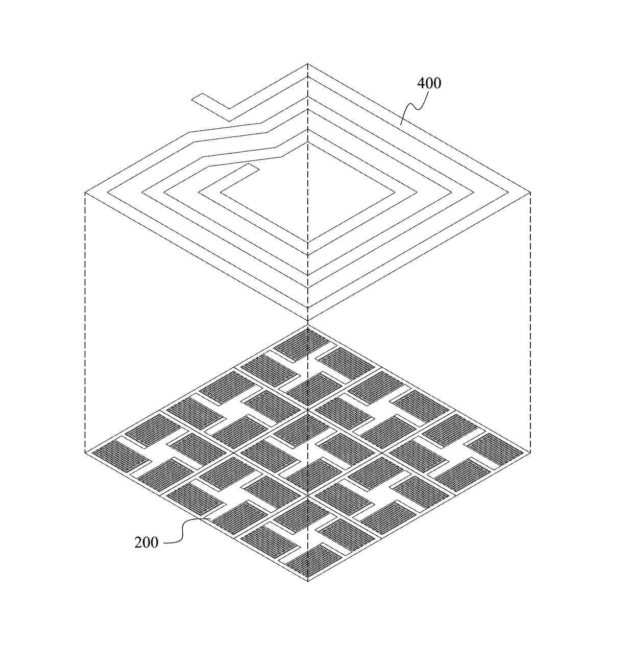
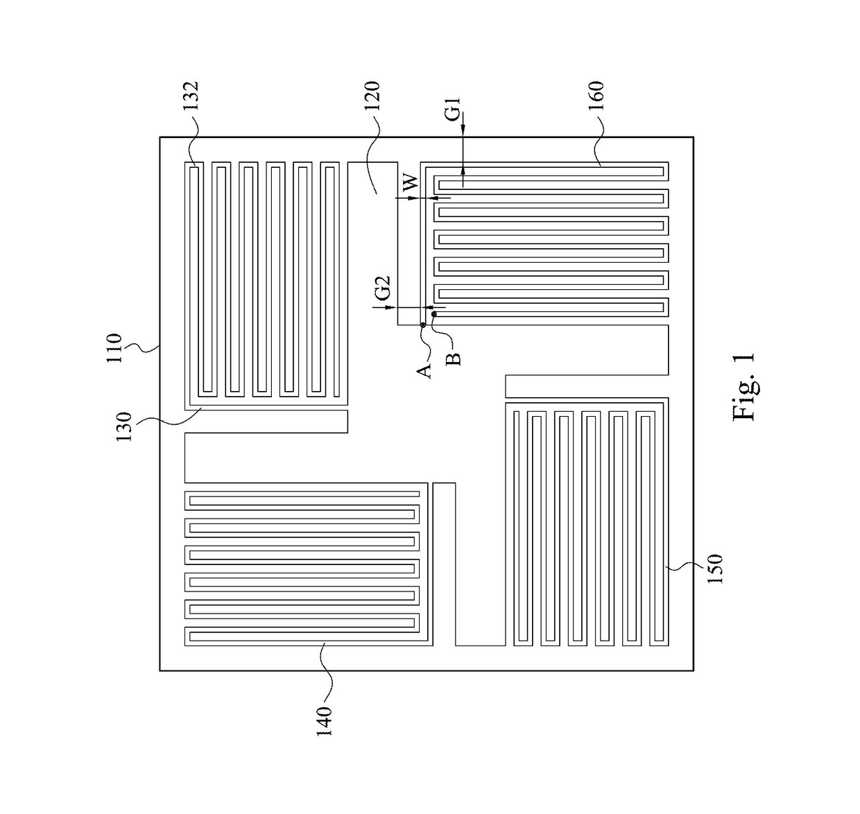
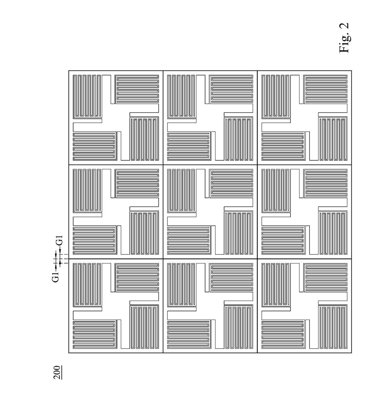
[0030]On the other hand, for the capacitance effect, if the anti-electromagnetic interference unit has M×N electromagnetic band gap structures, the distance between two electromagnetic band gap structures affects the capacitance value corresponded to the capacitance effect generated by the arrange shape of the electromagnetic band gap structures. In the present invention, each of the electromagnetic band gap structures is a square. The arrangement of the electromagnetic band gap structures is a rectangle. M pieces of the electromagnetic band gap structures are arranged at a first side of the rectangle, and N pieces of the electromagnetic band gap structures are arranged at a second side of the rectangle. M and N are positive integers, and an angle between the first side and the second side is 90 degree. Referring to FIG. 2, FIG. 2 is a plane structural diagram of 3×3 electromagnetic band gap structures arranging to each other according to the present invention. In the anti-electroma...
second embodiment
[0031]FIG. 3 is a plane structural diagram of 2×3 electromagnetic band gap structures arranging to each other according to the present invention. In the anti-electromagnetic interference unit 300 of FIG. 3, six electromagnetic band gap structures are arranged to each other. Two electromagnetic band gap structures are arranged in one side, and three electromagnetic band gap structures are arranged in another side. If G1 is smaller, the arrangement of the electromagnetic band gap structure is closer so as to generate the greater capacitance value corresponded to the capacitance effect. Similarly, according to the above formula (1), if the capacitance value is greater, the bandgap central frequency is lower. Therefore, through adjusting the capacitance effect generated by the arrangement shape of the 2×3 electromagnetic band gap structures, such as arranging the 2×3 electromagnetic band gap structures to be more closely, the bandgap central frequency f can be reduced.
[0032]FIG. 4 is a ...
PUM
 Abstract
Description
Claims
Application Information


