Electrostatic chuck device, and semiconductor manufacturing device

a technology of electrostatic chuck and semiconductor, which is applied in the direction of electrostatic holding device, manufacturing tools, metal-working machine components, etc., can solve the problems of difficult uniform control of heat transfer coefficient between the electrostatic chuck and the cooling base part, damage to the compositional components and high degree of adhesion deterioration, so as to prevent infiltration and suppress the deterioration of the adhesion layer due to plasma , the effect of uniform control

Active Publication Date: 2018-01-25
SUMITOMO OSAKA CEMENT CO LTD
View PDF0 Cites 10 Cited by
  • Summary
  • Abstract
  • Description
  • Claims
  • Application Information

AI Technical Summary

Benefits of technology

[0021]According to the present invention, in order to prevent infiltration of plasma entering through the through-hole, the inner insulator and the electrostatic chuck part inner peripheral surface are in contact with each other, or the adhesion layer extends in a gap between the inner insulator and the electrostatic chuck part inner peripheral surface, and the insulator has an insulator inner end face formed on the electrostatic chuck part side of the insulator main body, and an insulator outer end face formed on the electrostatic chuck part side of the insulator main body so as to face the electrostatic chuck part outer peripheral surface. For this reason, deterioration of the adhesion layer due to plasma can be suppressed, and therefore, it is possible to provide an electrostatic chuck device and a semiconductor manufacturing device, in which it is possible to more uniformly control the heat transfer coefficient between an electrostatic chuck part and a cooling base part.
[0022]Further, according to the present invention, in order to prevent infiltration of plasma entering through the through-hole, particularly, the electrostatic chuck part through-hole, the insulator inner end face and the elect...

Problems solved by technology

The adhesion layer between the electrostatic chuck part and the cooling base part in the through-hole is exposed to the plasma infiltrated into the through-hole, and thus the compositional components of the adhesion layer are subjected to damage or the like.
Therefore, there is a concern that consumption of the adhesion layer or det...

Method used


Image

  • Electrostatic chuck device, and semiconductor manufacturing device
  • Electrostatic chuck device, and semiconductor manufacturing device
  • Electrostatic chuck device, and semiconductor manufacturing device

Examples


first embodiment

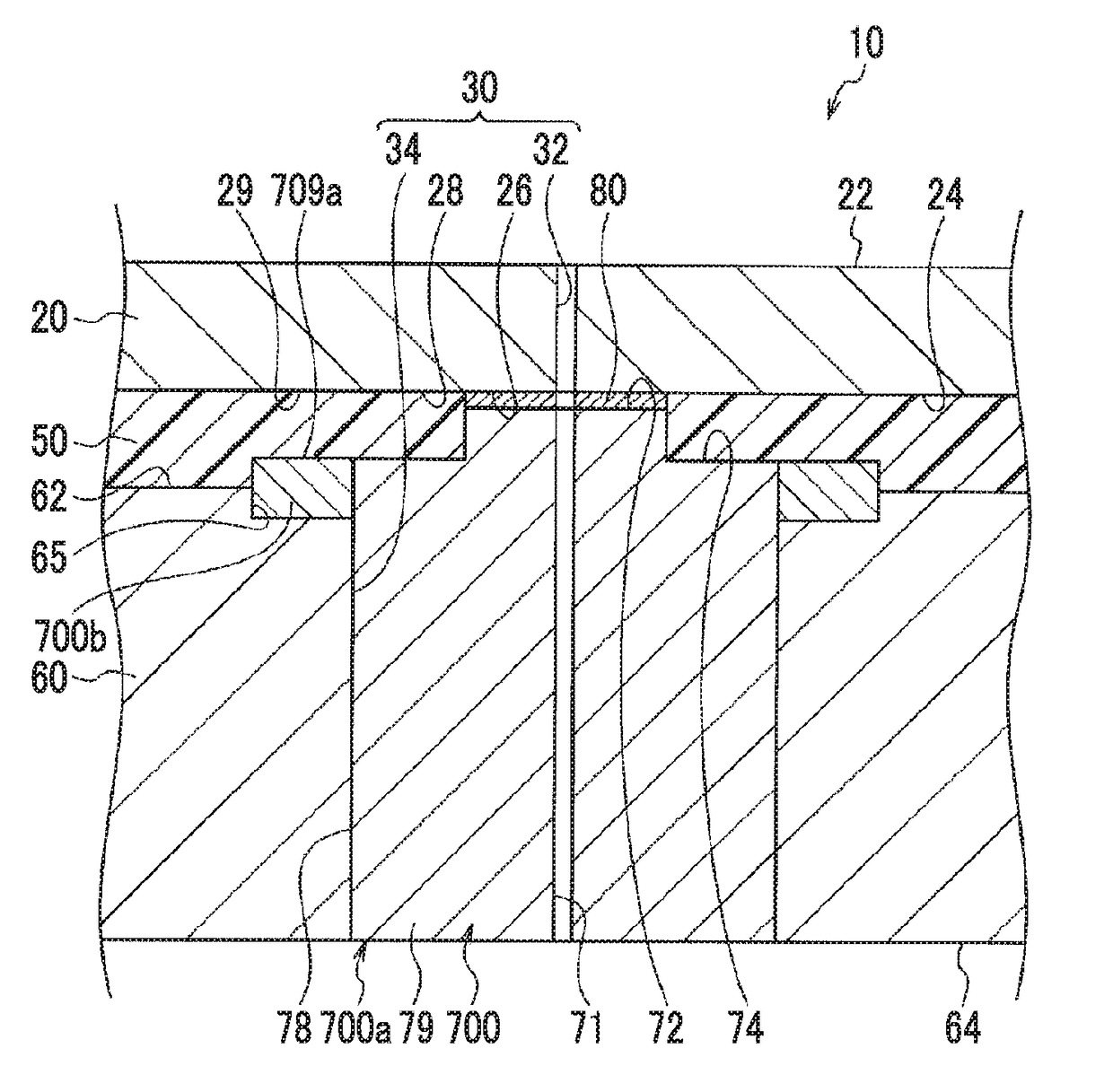
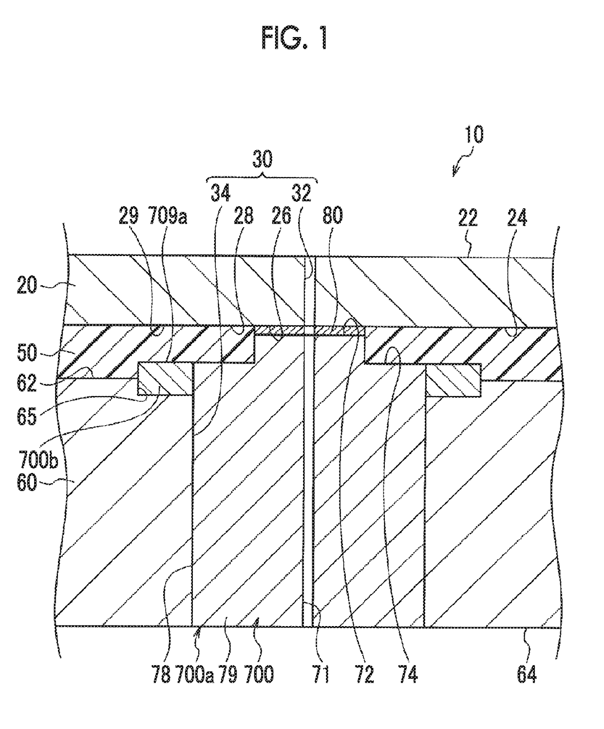
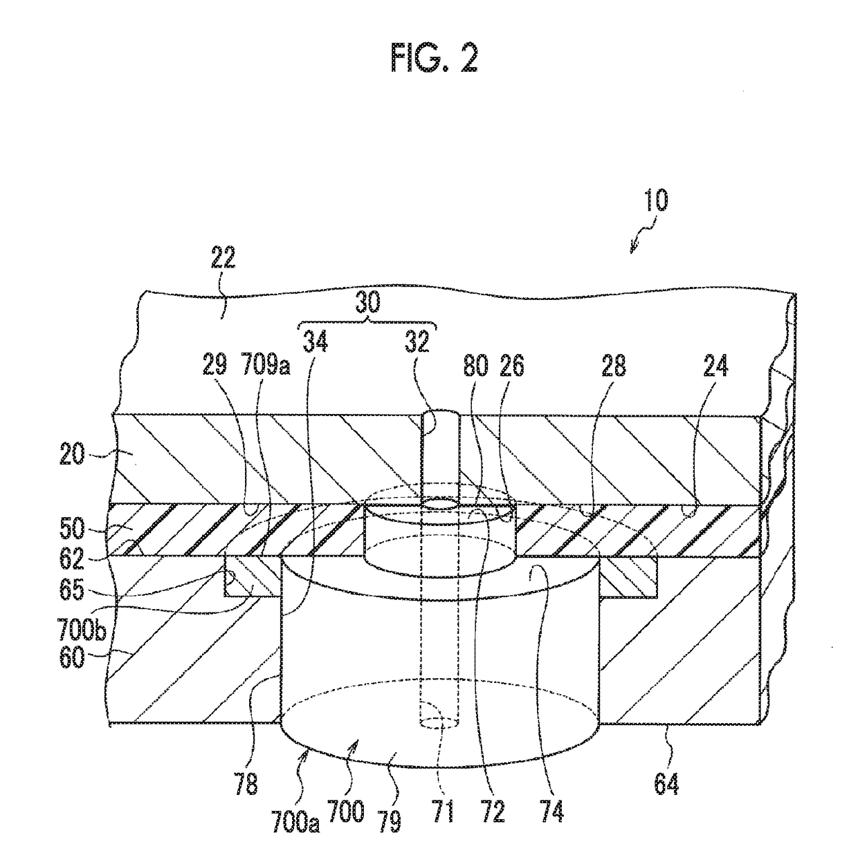
[0035]First, with respect to the first aspect of the present invention, the electrostatic chuck device 10 according to the present invention will be described with reference to FIGS. 1 and 2.

[0036]The electrostatic chuck device 10 is provided with an electrostatic chuck part 20, a cooling base part 60, an adhesion layer 50, a through-hole 30, and an insulator 700.

[0037]The electrostatic chuck part 20 is a plate-shaped member having one main surface 22 which is a surface on which a plate-shaped sample is placed, and the other main surface 24 which is a surface on the side opposite to one main surface 22.

[0038]The electrostatic chuck part 20 is formed of ceramic. Although not shown in the drawings, the electrostatic chuck part 20 has a placing plate, a supporting plate, an internal electrode for electrostatic attraction, and an insulating material layer.

[0039]One main surface 22 is a placing surface on which the plate-shaped sample is placed.

[0040]The other main surface 24 includes an...

second embodiment

[0070]Next, with respect to a second aspect of the present invention, an electrostatic chuck device 11 according to the present invention will be described with reference to FIG. 3.

[0071]The electrostatic chuck device 11 is the same as the electrostatic chuck device 10 except that the electrostatic chuck device 11 is further provided with the plasma-resistant adhesive layer 90.

[0072]The plasma-resistant adhesive layer 90 has a ring-shaped adhesive part 92. The ring-shaped adhesive part 92 is formed between the electrostatic chuck part outer peripheral surface 28 and the insulator outer end face 74 such that plasma infiltrating through the chuck part through-hole 32 does not erode the adhesion layer 50.

[0073]The plasma-resistant adhesive layer 90 is, for example, an acrylic or fluorine-based adhesive.

[0074]According to the electrostatic chuck device 11, the plasma-resistant adhesive layer 90 has the ring-shaped adhesive part 92, and therefore, the plasma-resistant adhesive layer 90 p...

third embodiment

[0076]An electrostatic chuck device 1 according to the present invention will be described with reference to FIGS. 4 and 5.

[0077]The electrostatic chuck device 1 is provided with the electrostatic chuck part 20, the cooling base part 60, the adhesion layer 50, the through-hole 30, an insulator 70, and the plasma-resistant adhesive layer 90.

[0078]The adhesion layer 50 is formed between the other main surface 24 of the electrostatic chuck part 20 and the upper surface 62 of the cooling base part 60 and bonds the electrostatic chuck part 20 and the cooling base part 60 together.

[0079]The base part through-hole 34 has a larger diameter than the chuck part through-hole 32 such that the electrostatic chuck part inner peripheral surface 26 and the electrostatic chuck part outer peripheral surface 28 are exposed from the base part through-hole 34.

[0080]The insulator 70 is the inner insulator 700a of the insulator 70 in the first and second embodiments and does not have the outer insulator 7...


PUM


Abstract

An electrostatic chuck part of an electrostatic chuck device has an electrostatic chuck part inner peripheral surface surrounding an opening of a chuck part through-hole, and an electrostatic chuck part outer peripheral surface surrounding the electrostatic chuck part inner peripheral surface. An insulator has an insulator main body in which an insulator through-hole having an opening on the electrostatic chuck part side is formed, an insulator inner end face, and an insulator outer end face which faces the electrostatic chuck part outer peripheral surface. The insulator inner end face and the electrostatic chuck part inner peripheral surface are in contact with each other, or an adhesion layer or a plasma-resistant adhesive layer extends in a gap between the insulator inner end face and the electrostatic chuck part inner peripheral surface. The plasma-resistant adhesive layer is formed between the electrostatic chuck part outer peripheral surface and the insulator outer end face.

Description

TECHNICAL FIELD[0001]The present invention relates to an electrostatic chuck device and a semiconductor manufacturing device.BACKGROUND ART[0002]Patent Literature No. 1 discloses that a semiconductor manufacturing device using plasma, such as a plasma etching device or a plasma CVD device is provided with an electrostatic chuck device for fixing a plate-shaped sample such as a wafer, and a plasma irradiation mechanism for irradiating the fixed plate-shaped sample with plasma.[0003]In the electrostatic chuck device, an adhesion layer is formed between an electrostatic chuck part having a placing surface on which a plate-shaped sample is placed and a cooling base part for cooling the electrostatic chuck part such that the electrostatic chuck part and the cooling base part are bonded together. Further, the electrostatic chuck device has a plurality of through-holes penetrating the electrostatic chuck part, the adhesion layer, and the cooling base part.[0004]Further, there is a case of ...

Claims


Application Information

Patent Timeline
IPC IPC(8): H01L21/683H01L21/67
CPCH01L21/6833H01L21/67103H01L21/67109H01L21/6831H01L21/68757H02N13/00B23Q3/15
Inventor ISHIMURA, KAZUNORIANDO, KAZUTOTAKAHASHI, KENTAROKINPARA, YUHKIMAETA, SHINICHIKOSAKAI, MAMORU
Owner SUMITOMO OSAKA CEMENT CO LTD
Why Eureka
Try Eureka