Display device and electronic device

Active Publication Date: 2018-01-25
SEMICON ENERGY LAB CO LTD
View PDF26 Cites 17 Cited by
  • Summary
  • Abstract
  • Description
  • Claims
  • Application Information

AI Technical Summary

Benefits of technology

[0007]In addition, when pixel circuits each including a transistor that constitutes a gate driver and pixel circuits without a transistor that constitutes a gate driver are provided in a mixed manner, the circuit design is more complex because two different kinds of pixel circuits are included. Similarly, wirings for connecting transistors that constitute a gate driver have different connection relations from each other, which is also problematic because it makes the circuit design more complex.
[0008]An object of one embodiment of the present invention is to provide a dis

Problems solved by technology

In that case, the pixel circuit including a transistor that constitutes a gate driver makes the area of a pixel larger, as compared with the pixel circuit without such a transistor, which is problematic because it hinders increase of resolution.
In addition, when pixel circuits each including a transistor that constitutes a gate driver and pixel circuits without a tra

Method used


Image

  • Display device and electronic device
  • Display device and electronic device
  • Display device and electronic device

Examples


embodiment 1

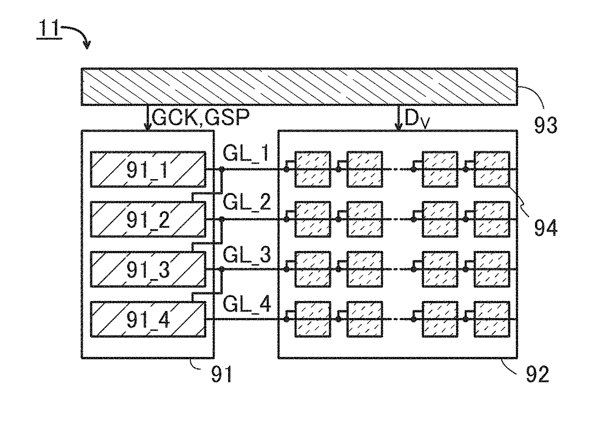
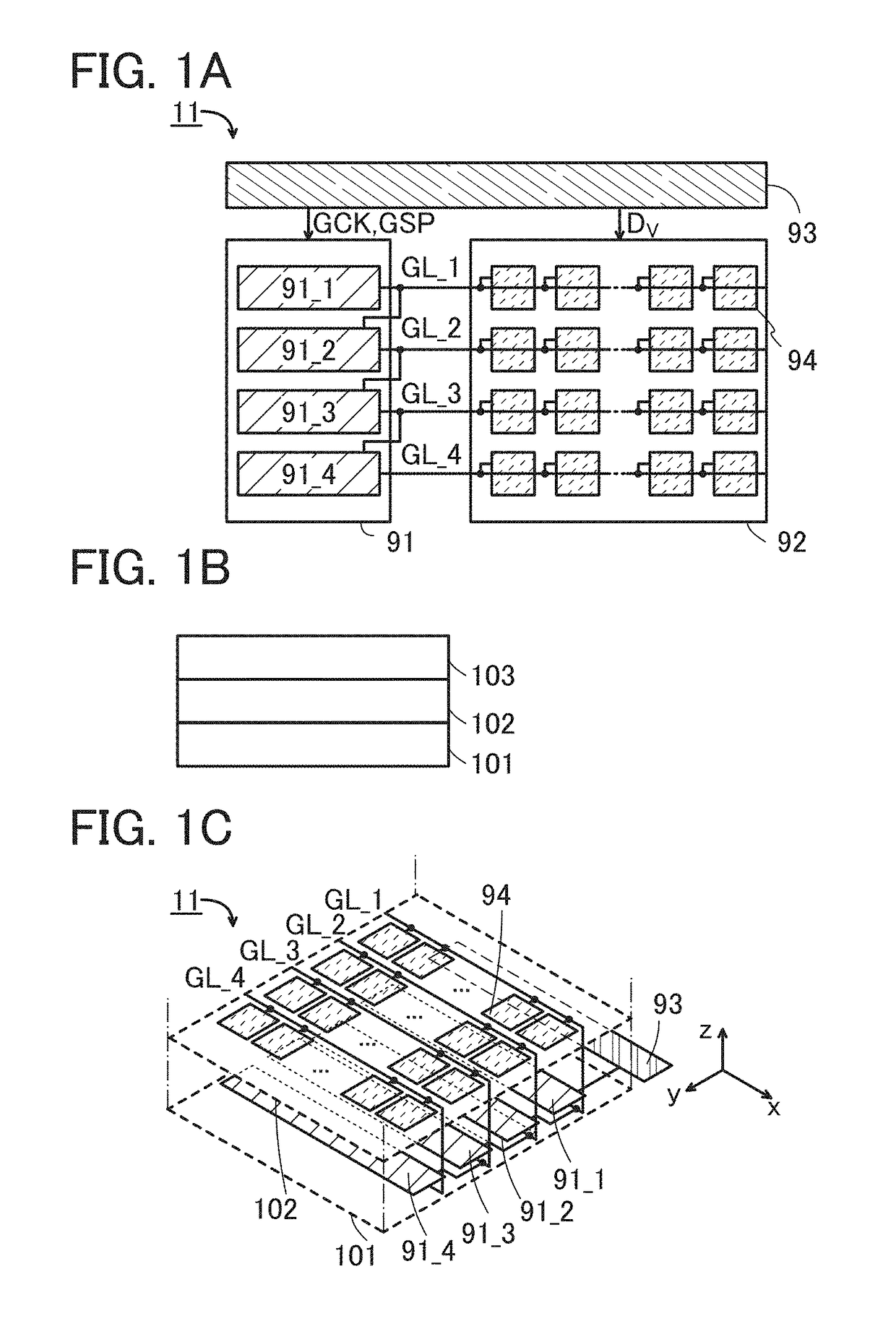
[0046]In a display portion of a display device of one embodiment of the present invention, a layer including transistors that constitute pixel circuits and a layer including transistors that constitute a driver circuit are stacked. That is, transistors that constitute pixel circuits are provided in an upper layer, and transistors that constitute a gate driver, which is a driver circuit, are provided in a lower layer. The gate driver, which is generally provided in a bezel portion, is provided in the lower layer in the display portion; whereby improvement in design flexibility such as a narrower bezel can be achieved. In addition, transistors that constitute pixel circuits are provided in the upper layer in the display portion, so that the upper layer is designed to have repetition of the same circuit layout; whereby the circuit design can be prevented from becoming complex.

[0047]A structure of the display device will be described with reference to the drawings.

[0048]FIG. 1A is a dra...

embodiment 2

[0097]In this embodiment, a display device that can be used for one embodiment of the present invention and a driving method thereof are described.

[0098]The display device of one embodiment of the present invention can include a pixel in which a first display element that reflects visible light is provided, a pixel in which a second display element that emits visible light is provided, a pixel in which a third display element that transmits visible light is provided, or a pixel in which the first display element and one of the second and third display elements are provided.

[0099]In this embodiment, a display device including a first display element that reflects visible light and a second display element that emits visible light is described.

[0100]The display device has a function of displaying an image utilizing one or both of first light reflected by the first display element and second light emitted from the second display element. Alternatively, the display device has a function...

embodiment 3

[0132]An example of a display panel that can be used for the display device of one embodiment of the present invention is described below. The display panel described below as an example includes both a reflective liquid crystal element and a light-emitting element and can display an image both in a transmissive mode and in a reflective mode.

[Structure Example]

[0133]FIG. 15A is a block diagram illustrating an example of the structure of a display device 400. The display device 400 includes a plurality of pixels 410 that are arranged in a matrix in a display portion 362. The display device 400 also includes a circuit GD and a circuit SD. In addition, the display device 400 includes a plurality of wirings G1, a plurality of wirings G2, a plurality of wirings ANO, and a plurality of wirings CSCOM, which are electrically connected to the circuit GD and the pixels 410 arranged in a direction R. Moreover, the display device 400 includes a plurality of wirings S1 and a plurality of wirings...


PUM


Abstract

A display device that can be easily and more flexibly designed is provided. The display device includes a pixel circuit and a driver circuit in a display portion. The driver circuit includes a plurality of pulse output circuits. Each of the plurality of pulse output circuits has a function of driving a gate line. The pixel circuit is electrically connected to the gate line. Each of the plurality of pulse output circuits includes a first transistor. The pixel circuit includes a second transistor. A layer including the second transistor is over a layer including the first transistor, and the first transistor and the second transistor overlap with each other.

Description

BACKGROUND OF THE INVENTION1. Field of the Invention[0001]The present invention relates to an object, a method, or a manufacturing method. The present invention relates to a process, a machine, manufacture, or a composition of matter. Specifically, one embodiment of the present invention relates to a semiconductor device, a light-emitting device, a display device, an electronic device, a lighting device, a driving method thereof, or a manufacturing method thereof. In particular, one embodiment of the present invention relates to a display device (display panel). Another embodiment of the present invention relates to an electronic device, a light-emitting device, or a lighting device that includes a display device, or a manufacturing method thereof.[0002]In this specification and the like, a semiconductor device generally refers to a device that can function by utilizing semiconductor characteristics. A transistor, a semiconductor circuit, an arithmetic device, a memory device, and t...

Claims


Application Information

Patent Timeline
IPC IPC(8): H01L51/50H01L51/05
CPCH01L51/502H01L51/0512G02F1/136286G06F1/1601H01L51/504G09G3/2003G09G3/3225G09G3/3413G09G3/3426G09G3/3648G09G2300/023G09G2300/0456G09G2310/0286G09G2320/0666G09G2320/0686G09G2360/144H10K59/1213G09G3/3266G09G2300/0439G09G2300/046G09G2300/0809G09G2300/0426G09G3/3233G09G2300/0842
Inventor KOBAYASHI, HIDETOMOTOYOTAKA, KOUHEI
Owner SEMICON ENERGY LAB CO LTD
Why Eureka
Try Eureka