Organic el display panel and method of manufacturing organic el display panel

Active Publication Date: 2018-02-15
JOLED INC
View PDF19 Cites 6 Cited by
  • Summary
  • Abstract
  • Description
  • Claims
  • Application Information

AI Technical Summary

Benefits of technology

[0011]According to the organic EL display panel relating to the aspect of the present disclosure, it is possible to suppress a

Problems solved by technology

In the case of an organic EL display panel in which a light shielding layer is carried on a color filter substrate that opposes a display element substrate, a position shift occurring at the time of alignment for sealing between the color filter substrate and the display element substrate, leading to outer edges of reflective electrode layers protruding from a light sh

Method used


Image

  • Organic el display panel and method of manufacturing organic el display panel
  • Organic el display panel and method of manufacturing organic el display panel
  • Organic el display panel and method of manufacturing organic el display panel

Examples


Example

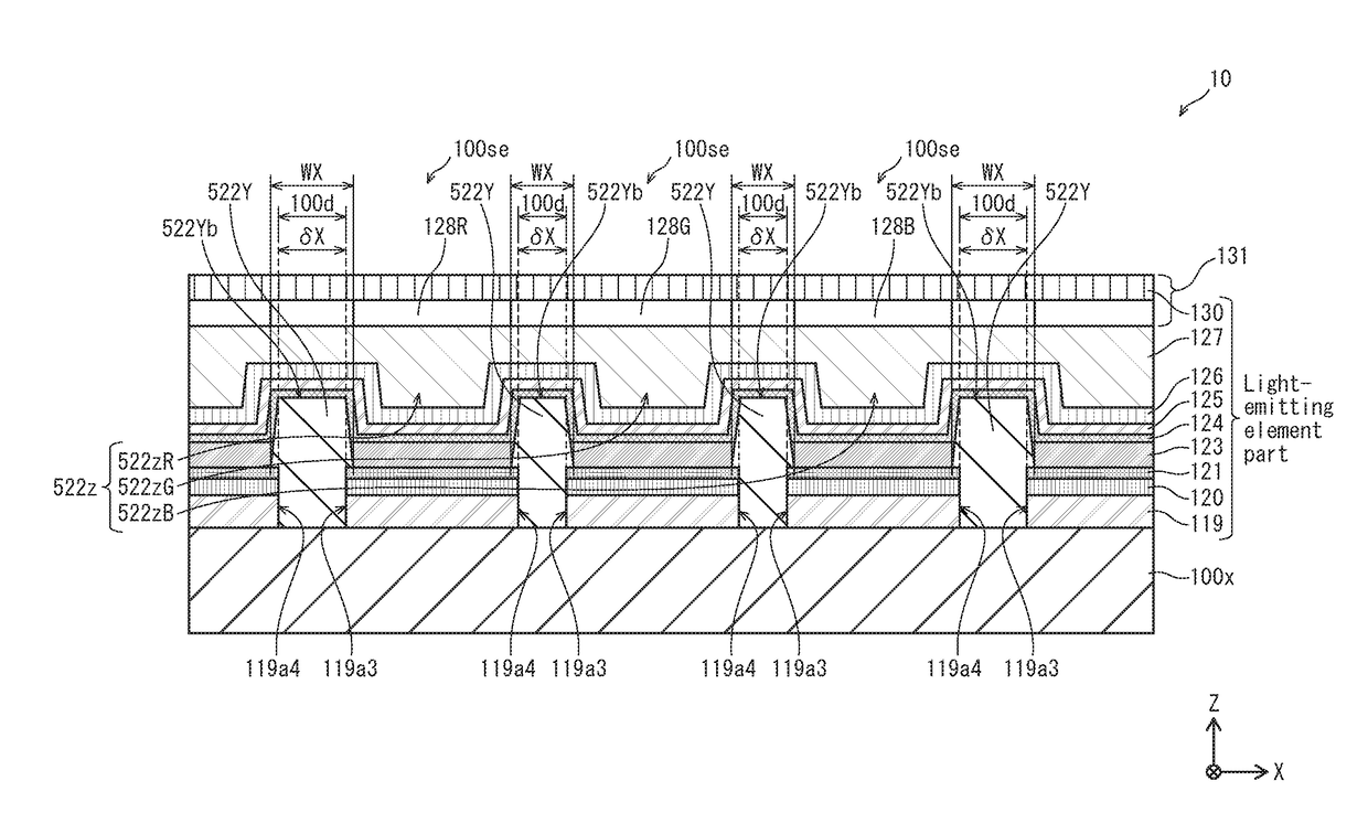
[0162]In the display panel 10 relating to Embodiment 1, the insulating layer 122 has a so-called line shape. Specifically, the column insulating sublayers 522Y are each formed above the outer edges in the row direction of two pixel electrode layers 119 that are adjacent in the row direction. The row insulating sublayers 122X extending in the row direction are each arranged in the column direction above the outer edges of two pixel electrode layers 119 that are adjacent in the column direction and above a region between the outer edges. The column insulating sublayers 522Y and the row insulating sublayers 122X are perpendicular to each other to constitute the insulating layer 122 having a lattice shape.

[0163]However, the insulating layer 122 only needs to be formed above the row and column outer edges of the pixel electrode layers 119, and the shape of the insulating layer 122 may be appropriately modified.

[0164]In an organic EL display panel 10A relating to Embodiment 2, a plurality...

Example

Embodiment 3

[0184]In the display panel 10 relating to Embodiment 1, the pixel electrode layers 119 are arranged on the substrate 100x in a matrix with the row interval δX therebetween and the column interval δY therebetween. Furthermore, the insulating layer 122 is formed so as to cover the pixel electrode layers 119. The inter-regions 100c, which have a length in the column direction between each two adjacent pixel electrode layers 119 corresponding to the column interval δY, have an area that is 30% or less of the area of the self-luminous regions 100a.

[0185]However, the insulating layer 122 only needs to be formed above the row and column outer edges of the pixel electrode layers 119, and the length of the column interval δY may be appropriately modified.

[0186]In an organic EL display panel 10B relating to Embodiment 3, a column interval δY between each two pixel electrode layers 119B covered with row insulating sublayers 122BX is substantially equal to the length of the pixel e...


PUM


Abstract

An organic electroluminescence (EL) display panel including pixels arranged in a matrix, the organic EL display panel includes: a substrate; pixel electrode layers made of a light-reflective material and arranged on the substrate in a matrix; an insulating layer provided at least above row and column outer edges of the pixel electrode layers and above inter-regions on the substrate between the row and column outer edges; an organic functional layer provided above the pixel electrode layers; and a counter electrode layer made of a light-transmissive material and is provided above the organic functional layer, wherein the organic functional layer includes light-emitting layers that are provided in regions above the pixel electrode layers where the insulating layer is not provided, the light-emitting layers causing organic electroluminescence, and the insulating layer has an optical density of 0.5 to 1.5 in a direction of the substrate when viewed in plan.

Description

[0001]This application is based on an application No. 2016-157862 filed in Japan, the contents of which are hereby incorporated by reference.BACKGROUND OF THE DISCLOSURE(1) Technical Field[0002]The present disclosure relates to organic electroluminescence (EL) display panels that use organic EL elements that make use of electroluminescence of organic material, and to a method of manufacturing the same.(2) Description of Related Art[0003]In recent years, as display panels used in display devices such as digital televisions, organic EL display panels are being implemented in which a plurality of organic EL elements are arrayed in a matrix on a substrate. Such organic EL display panels have high visibility, because each organic EL element is self-luminous.[0004]In an organic EL display panel, each organic EL element has a basic structure in which a light-emitting layer containing an organic light-emitting material is disposed between an anode and cathode electrode pair, and when driven...

Claims


Application Information

Patent Timeline
IPC IPC(8): H01L27/32H01L51/00H01L51/52
CPCH01L27/3246H01L51/5218H01L51/0097H01L27/322H01L2227/323H01L27/3248H01L2251/5315H01L2251/5338H01L27/3272Y02E10/549Y02P70/50H10K59/122H10K50/818H10K59/38H10K59/123H10K59/126H10K77/111H10K59/35H10K59/173H10K59/1201H10K2102/311H10K2102/3026
Inventor ABE, KAORUOSAKO, TAKASHINENDAI, KENICHI
Owner JOLED INC
Why Eureka
Try Eureka