Patterned-illumination systems adopting a computational illumination

a computational illumination and patterned illumination technology, applied in the field of illumination, can solve the problems of limiting the practical use of patterned illumination imaging modalities, existing structured illumination techniques that require expensive optical or mechanical devices, and achieve the effect of improving resolution imaging

Inactive Publication Date: 2018-02-15
RGT UNIV OF CALIFORNIA
View PDF6 Cites 31 Cited by
  • Summary
  • Abstract
  • Description
  • Claims
  • Application Information

AI Technical Summary

Benefits of technology

[0011]The disclosed technology overcomes a number of issues that significantly hinder the practical use of patterned illumination imaging modalities. In the presented technology an illumination pattern-shift can be achieved on the object plane by simply switching between illumination patterns with the use of simple computational illumination hardware without mechanically switching the patterns and / or the light source. It is also possible to shift the desired patterns by simply replacing the light source with the disclosed computational illumination hardware, which in a preferred embodiment is a lenseless system consisting of a significantly simpler optical setup. In addition, it is possible to smoothly shift a pattern at its maximum resolution without limitation of the illumination imaging system numerical aperture and / or other active devices.
[0013]This simple hardware implementation enables any imaging technique relevant to pattern shifting by turning on different LEDs on the array. The disclosure describes how the illumination pattern, e.g., grating image, can be shifted by the presented method and demonstrates several different patterned-illumination imaging techniques using this setup, including phase retrieval, super-resolution imaging and a variation of Fourier Ptychography. In addition to the LED array setup, the same method can easily be applied to other computational illumination systems, such as a combination of single light source that is moving or patterned with Spatial Light Modulators (SLMs), deformable mirror devices (DMDs) or Liquid Crystal Displays (LCDs).
[0014]Numerous advantages and improvements are provided over prior technology, such as exemplified in the following. (a) Existing structured illumination techniques require expensive (greater than $1000) optical or mechanical devices, such as SLMs, DMDs, or piezo translation stages. With the disclosed computational illumination for pattern-shifting, only a low resolution programmable light source and a coded mask are needed to replace the lamp inside the microscope. This computational illumination hardware (e.g., an LED array) is very inexpensive at about $100 compared to existing systems and can be readily implemented into existing microscopes without extra hardware. In addition, the speed of the disclosed programmable illumination hardware (LED array) can be extremely fast and suitable for real-time imaging applications.
[0015](b) The disclosed technique uses computational illumination to shift the pattern on the imaging plane without physical movement of any component, which is important especially for sensitive objects and small working distances. It does not suffer the hysteresis and repeatability problems of mechanical motion, nor is it polarization sensitive like many SLMs are. Phase patterned masks may be used in order to avoid any loss of photons through the system and make the light throughput better than competing methods.
[0017](d) The resolution of the patterned mask is important when conducting structured illumination microscopy. The existing movable patterned mask generated by the light interference using SLM or DMD is focused through an imaging system, which imposes a resolution constraint (finite NA) on the patterned mask image. The disclosed technique does not re-image the pattern and shifts the mask pattern through propagation, which does not affect the resolution of the patterned mask image. Thus, a patterned mask with features much smaller than the resolution limit of the system can be used to achieve enhanced resolution imaging.
[0018](e) Because the pattern shifting is achieved by moving the source instead of the pattern itself, and the source-to-pattern distance is generally much larger than the pattern-to-sample distance, the step size requirements for source stepping are much less stringent than they are for pattern stepping, significantly reducing the need for precise shifting. The shift and the pattern itself at the sample can be tuned by choosing the patterned mask-to-sample distance or source-to-pattern distance appropriately.

Problems solved by technology

The disclosed technology overcomes a number of issues that significantly hinder the practical use of patterned illumination imaging modalities.
(a) Existing structured illumination techniques require expensive (greater than $1000) optical or mechanical devices, such as SLMs, DMDs, or piezo translation stages.

Method used


Image

  • Patterned-illumination systems adopting a computational illumination
  • Patterned-illumination systems adopting a computational illumination
  • Patterned-illumination systems adopting a computational illumination

Examples


Embodiment Construction

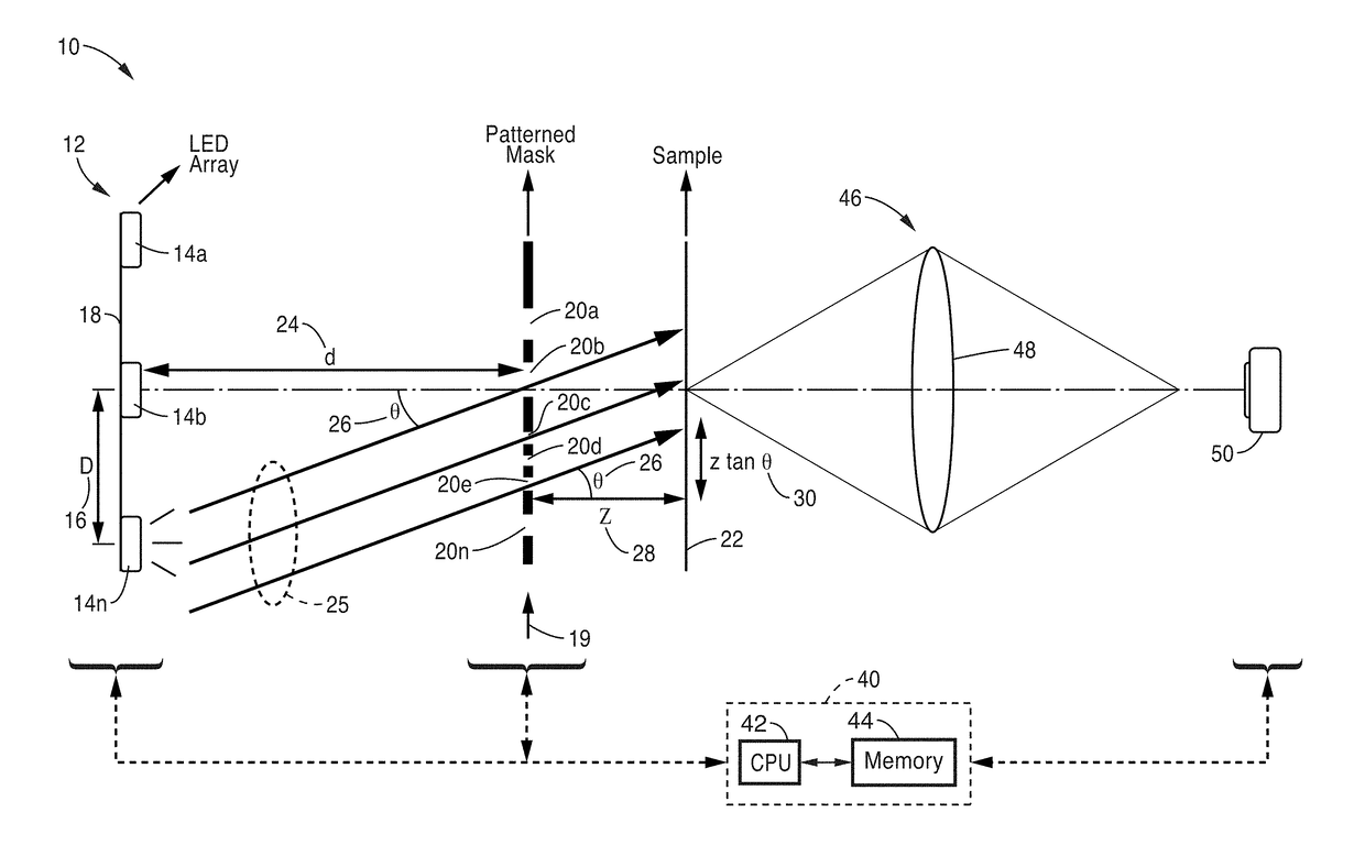
[0029]1. Illumination Pattern Shift Using An LED Array

[0030]The concept of the disclosed patterned-illumination system adopting computational illumination, is exemplified in the following illustrations.

[0031]FIG. 1 illustrates an embodiment 10 of illumination pattern shifting using an array of optical elements, herein generally exemplified as a light emitting diode (LED) array 12, although other optical sources may be utilized without departing from the teachings of the disclosure. LED array 12 is shown with LEDs 14a, 14b, through 14n spaced a distance 16 (D) along a backplane 18. In this example LEDs 14a, 14b are shown non-active (not optically emitting) while LED 14n is actively outputting light. It will be appreciated that for the sake of simplicity of illustration, a single axis of LEDs is depicted, while in typical applications, the LED array would be implemented as a planar two-dimensional array.

[0032]The LED array 12 is placed sufficiently far away 24 (d) from the patterned m...


PUM


Abstract

A method and apparatus for increasing sample image resolution using patterned illumination. An array of optical emitters is selectively activated as a programmable light source, directed to a patterned mask which selectively changes amplitude or phase characteristics of optical energy received onto a sample. A sequence of images are captured of the sample, each being captured in response to a different spatial arrangement of optical outputs from the optical emitter array. These sample images are then post processed into a reconstructed image which has increased resolution over the separately collected images of the sample.

Description

CROSS-REFERENCE TO RELATED APPLICATIONS[0001]This application is a 35 U.S.C. §111(a) continuation of PCT international application number PCT / US2016 / 015701 filed on Jan. 29, 2016, incorporated herein by reference in its entirety, which claims priority to, and the benefit of, U.S. provisional patent application Ser. No. 62 / 109,240 filed on Jan. 29, 2015, incorporated herein by reference in its entirety. Priority is claimed to each of the foregoing applications.[0002]The above-referenced PCT international application was published as PCT International Publication No. WO 2016 / 123508 on Aug. 4, 2016, which publication is incorporated herein by reference in its entirety.STATEMENT REGARDING FEDERALLY SPONSORED RESEARCH OR DEVELOPMENT[0003]This invention was made with Government support under 1351896 awarded by the National Science Foundation. The Government has certain rights in the invention.INCORPORATION-BY-REFERENCE OF COMPUTER PROGRAM APPENDIX[0004]Not ApplicableNOTICE OF MATERIAL SUB...

Claims


Application Information

Patent Timeline
Patent Type & Authority Applications(United States)
IPC IPC(8): H04N5/232H04N5/235G02B21/36H04N5/225G02B21/06G02B27/58
CPCH04N5/23232G02B21/06G02B27/58G02B21/367H04N5/2256H04N5/2354G01B11/2513H04N23/56H04N23/951H04N23/74
Inventor WALLER, LAURACHEN, MICHAELYEH, LI-HAO
Owner RGT UNIV OF CALIFORNIA
Why Eureka
Try Eureka