Electronic package and method for fabricating the same

a technology of electronic packaging and packaging elements, applied in the direction of semiconductor devices, semiconductor/solid-state device details, electrical apparatus, etc., can solve the problems of imbalanced contact stress and sloped coupling between the first and the second package, poor electrical connections, and complicated fabrication process of the traditional semiconductor package b>1/b>, so as to prevent contact offset, good electrical connections, and good coplanarity of the grid array

Inactive Publication Date: 2018-03-08
SILICONWARE PRECISION IND CO LTD
View PDF5 Cites 4 Cited by
  • Summary
  • Abstract
  • Description
  • Claims
  • Application Information

AI Technical Summary

Benefits of technology

[0017]It can be seen from the above that in an electronic package and a method for fabricating the same according to the present disclosure, the electronic component is bonded onto the first carrier structure via the bonding layer, and thus the distance between the first carrier structure and the second carrier structure can be fixed. Compared to the prior art, contacts formed by the conductive elements after the conductive elements are reflowed according to the present disclosure, are able to maintain good electrical connections, and good coplanarity of the grid array formed by the conductive elements can be achieved, resulting in balanced contact stress and no sloped coupling between the first and second carrier structures, thereby preventing contact offset.
[0018]Moreover, the method for fabricating an electronic package according to the present disclosure requires only one flux cleaning process, which reduces the number of flux cleaning processes, thereby simplifying the manufacturing processes, reducing production cost and increasing product yield.

Problems solved by technology

The tolerances of the volume and height of the conductive elements 18 after reflow are large, which not only result in flawed contacts that lead to poor electrical connections, but poor coplanarity of the grid array formed by these conductive elements 18, which leads to imbalanced contact stress and sloped coupling between the first and the second package substrates 10 and 12, or even contact offset.
Furthermore, the fabrication process of the traditional semiconductor package 1 is rather complex (e.g., requiring two flux cleaning procedures) and the production cost is higher.

Method used


Image

  • Electronic package and method for fabricating the same
  • Electronic package and method for fabricating the same
  • Electronic package and method for fabricating the same

Examples


Embodiment Construction

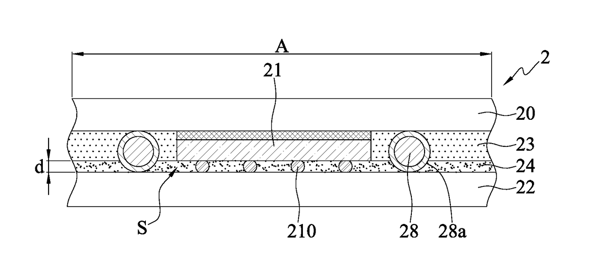
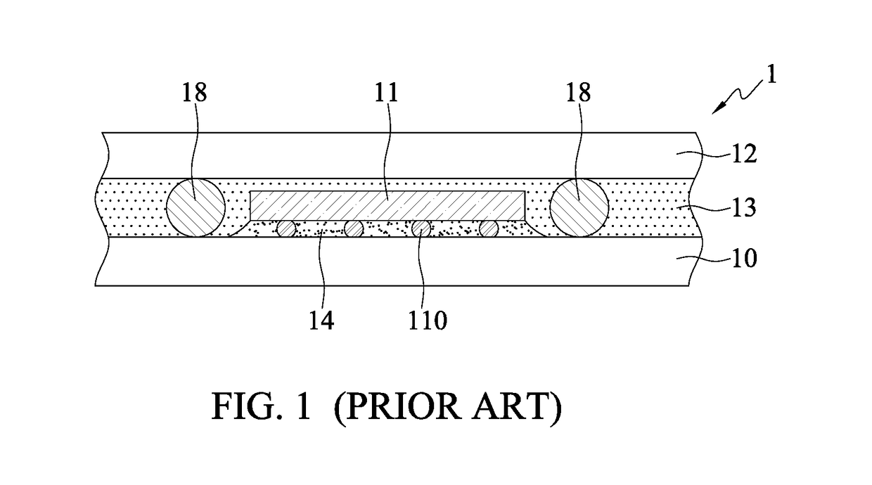
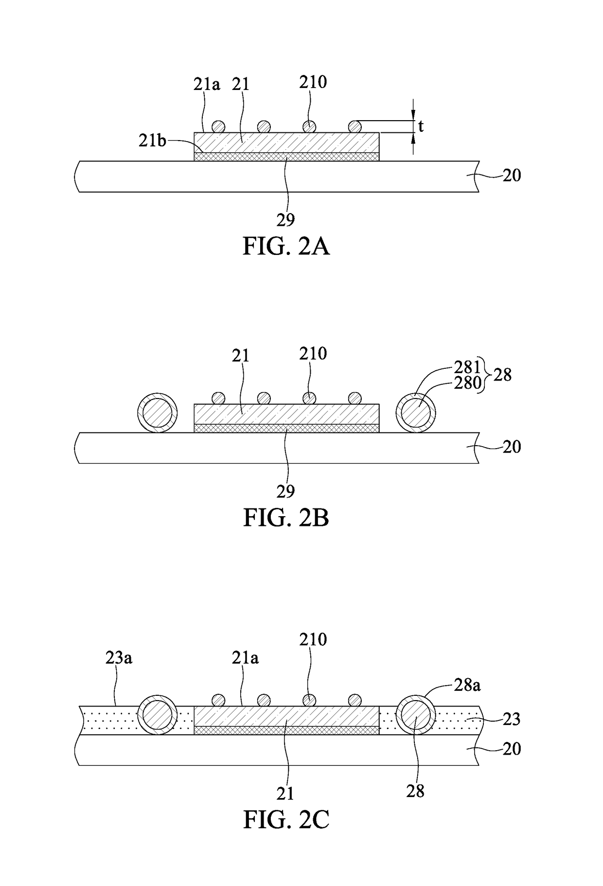
[0022]The present disclosure is described by the following specific embodiments. Those with ordinary skills in the arts can readily understand other advantages and functions of the present disclosure after reading the disclosure of this specification. The present disclosure may also be practiced or applied with other different implementations. Based on different contexts and applications, the various details in this specification can be modified and changed without departing from the spirit of the present disclosure.

[0023]It should be noted that the structures, ratios, sizes shown in the drawings appended to this specification are to be construed in conjunction with the disclosure of this specification in order to facilitate understanding of those skilled in the art. They are not meant, in any ways, to limit the implementations of the present disclosure, and therefore have no substantial technical meaning. Without affecting the effects created and objectives achieved by the present ...


PUM


Abstract

The present disclosure provides an electronic package and a method for fabricating the same. The method including: connecting a first carrier structure with an electronic component via a bonding layer formed thereon; stacking the first carrier structure on a second carrier structure via a plurality of conductive elements; and electrically connecting the electronic component to the second carrier structure to thereby maintain and secure the distance between the first and second carrier structures.

Description

BACKGROUND1. Technical Field[0001]The present disclosure relates to package structures, and, more particularly, to an electronic package and a method for fabricating the same.2. Description of Related Art[0002]With the rapid development of portable electronic products in the recent years, products are trending toward higher density, higher performance, more compact and lighter. In order to accommodate the demands for smaller form factors and higher density, the semiconductor industry has developed an array of package-on-package (PoP) technologies.[0003]As shown in FIG. 1, a method for fabricating a traditional PoP semiconductor package 1 involves bonding a semiconductor chip 11 onto a first package substrate 10 via a plurality of solder bumps 110 in a flip-chip manner, the solder bumps 110 are reflowed, and a first flux cleaning operation is performed. Then, an underfill 14 is applied to encapsulate the solder bumps 110. Thereafter, a second package substrate 12 is supported by and ...

Claims


Application Information

Patent Timeline
Patent Type & Authority Applications(United States)
IPC IPC(8): H01L21/48H01L25/065H01L23/00H01L21/56
CPCH01L21/4864H01L25/0657H01L24/29H01L24/13H01L21/563H01L24/83H01L2225/06517H01L2225/0652H01L2224/13147H01L21/50H01L23/31H01L24/11H01L23/3121H01L21/56H01L2225/06568H01L2224/92242H01L2224/81011H01L23/49816H01L23/49833H01L24/16H01L24/32H01L24/81H01L24/92H01L24/97H01L2224/16227H01L2224/2919H01L2224/32225H01L2224/32245H01L2224/81815H01L2224/83101H01L2224/97H01L2924/15321H01L2224/131H01L2224/81H01L2224/83H01L2924/00014H01L2924/014
Inventor TSAI, KUO-CHINGLIANG, JAU-ENCHEN, HSIN-LONG
Owner SILICONWARE PRECISION IND CO LTD
Why Eureka
Try Eureka