Semiconductor Devices Having Reduced Contact Resistance

a technology of contact resistance and semiconductor devices, applied in semiconductor devices, semiconductor/solid-state device details, electrical devices, etc., can solve the problems that the contact resistance between the source/drain region and the contact plug connected to the source/drain region may affect the characteristics of the device, and achieve the effect of reducing the contact resistan

Active Publication Date: 2018-03-29
SAMSUNG ELECTRONICS CO LTD
View PDF3 Cites 279 Cited by
  • Summary
  • Abstract
  • Description
  • Claims
  • Application Information

AI Technical Summary

Problems solved by technology

According to reductions in the size thereof, contact resistance between source / drain regions and contact plugs connected to source / drain regions may affect the characteristics of devices due to parasitic resistance of the semiconductor devices

Method used


Image

  • Semiconductor Devices Having Reduced Contact Resistance
  • Semiconductor Devices Having Reduced Contact Resistance
  • Semiconductor Devices Having Reduced Contact Resistance

Examples


Embodiment Construction

[0020]Hereinafter, embodiments of the present inventive concepts will be described as follows with reference to the attached drawings.

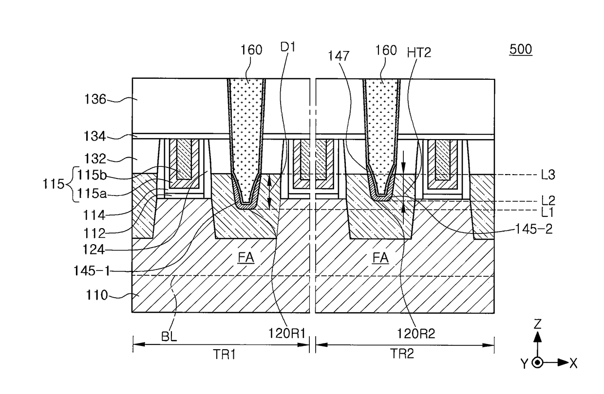
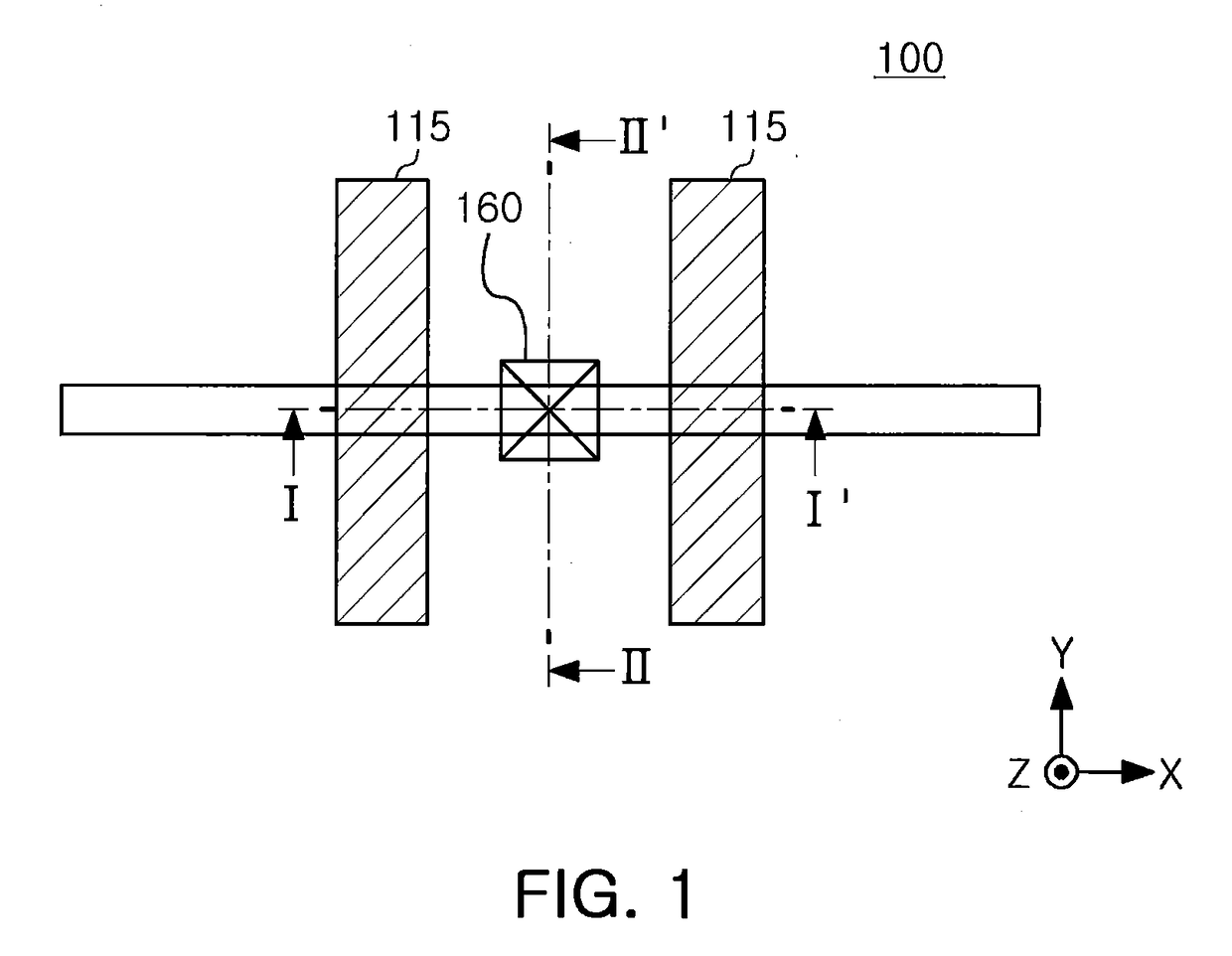
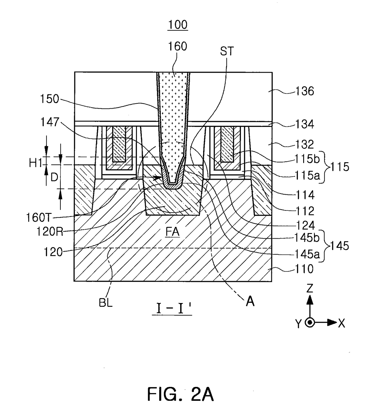
[0021]FIG. 1 is a layout of a semiconductor device according to an example embodiment of the present inventive concepts, while FIGS. 2A and 2B are cross-sectional views taken along line I-I′ and II-II′ of the semiconductor device of FIG. 1, respectively. FIG. 2C is a partially enlarged view of a portion ‘A’ of the semiconductor device of FIG. 2A. FIG. 3 is a perspective view of main components of the semiconductor device illustrated in FIGS. 2A and 2B

[0022]With reference to FIGS. 2A, 2B, 2C and 3 along with FIG. 1, a semiconductor device 100 may include a substrate 110 having a fin-type active region FA.

[0023]The substrate 110 may include a semiconductor, such as silicon (Si) or germanium (Ge), or a compound semiconductor, such as, for example, silicon germanium (SiGe), silicon carbide (SiC), gallium arsenide (GaAs), indium arsenide (InAs), and indium...


PUM


Abstract

A semiconductor device includes a substrate including an active region, a gate structure, source / drain regions, ones of the source / drain regions having an upper surface in which a recessed region is formed, a contact plug on the source / drain regions and extending in a direction substantially perpendicular to an upper surface of the substrate from an interior of the recessed region, a metal silicide film on an internal surface of the recessed region and including a first portion between a bottom surface of the recessed region and a lower surface of the contact plug and a second portion between a side wall of the recessed region and a side surface of the contact plug, and a metal layer connected to an upper portion of the metal silicide film and on a side surface of a region of the contact plug.

Description

CROSS-REFERENCE TO RELATED APPLICATION[0001]This U.S. non-provisional patent application claims priority under 35 U.S.C. § 119 to Korean Patent Application No. 10-2016-0124959 filed on Sep. 28, 2016, in the Korean Intellectual Property Office, the entire content of which is incorporated herein by reference.BACKGROUND1. Field[0002]The present inventive concepts relate to semiconductor devices and to methods of manufacturing semiconductor devices.2. Description of Related Art[0003]Due to an increase in demand for high-performance, high-speed semiconductor devices and / or multifunctional semiconductor devices, a degree of integration in semiconductor devices has increased. In order to manufacture semiconductor devices having a fine pattern in response to the increased integration in semiconductor devices, patterns having relatively narrow widths or short separation distances are desired. In order to overcome the limitations of planar metal oxide semiconductor FETs (MOSFETs), semiconduct...

Claims


Application Information

Patent Timeline
Patent Type & Authority Applications(United States)
IPC IPC(8): H01L29/45H01L23/535H01L29/08H01L29/78H01L29/06H01L29/417H01L21/768H01L29/66
CPCH01L29/45H01L23/535H01L29/0847H01L29/7851H01L29/66545H01L29/41791H01L21/76897H01L29/66795H01L29/0649H01L21/823821H01L21/845H01L29/785H01L27/0924H01L27/1211H01L29/401H01L29/665H01L21/28518H01L23/485H01L21/76805H01L21/76843H01L21/76855H01L29/41766H01L29/66348H01L21/32051
Inventor CHOI, HYO SEOKTOMITA, RYUJILEE, JOON GONKIM, CHUL SUNGLEE, JAE EUN
Owner SAMSUNG ELECTRONICS CO LTD
Why Eureka
Try Eureka