Width Adjustment of Stacked Nanowires

a nanowire and nanowire technology, applied in the direction of semiconductor devices, electrical devices, transistors, etc., can solve the problems of reducing the inability to achieve the configuration of devices using current processing technology, and achieve the effect of adjusting the effective device width of stacked nanowire devices

Inactive Publication Date: 2018-03-29
IBM CORP +1
View PDF3 Cites 47 Cited by
  • Summary
  • Abstract
  • Description
  • Claims
  • Application Information

AI Technical Summary

Problems solved by technology

One drawback to the stacked nanowire design is that the minimum device width is the periphery of each of one nanowire stack.
Such a device configuration cannot be achieved using current processing technology.

Method used


Image

  • Width Adjustment of Stacked Nanowires
  • Width Adjustment of Stacked Nanowires
  • Width Adjustment of Stacked Nanowires

Examples


Embodiment Construction

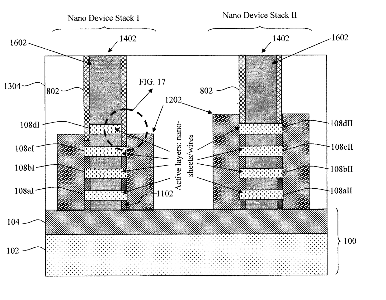
[0026]Provided herein are techniques for tuning the effective device width of stacked nanowires in a semiconductor device by cutting the top semiconductor nanowire(s) in a stack, making them not connected to the source / drain. As will be described in detail below, this device width tuning is achieved via a cut process post dummy gate formation, but before spacer deposition.

[0027]The effective width is essentially the width of the device that delivers the current. For nanowires, the effective width is the total conducting surface around the periphery of each wire. Here a goal is to be able to produce devices that operate with different current levels, which is achieved by modifying the effective device width.

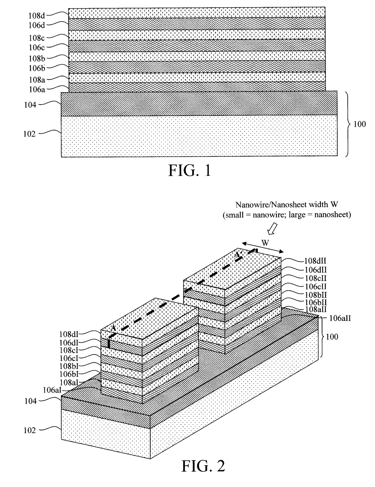
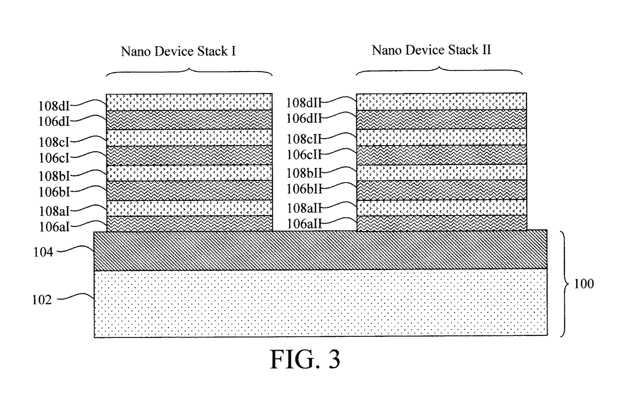
[0028]The present techniques will now be described by way of reference to FIGS. 1-15 which illustrate a process for forming a nanowire device having a variable device width. Namely, by way of the present process, the device width can be selectively tuned to produce devices having ...


PUM


Abstract

In one aspect, a method of forming a semiconductor device includes the steps of: forming an alternating series of sacrificial / active layers on a wafer and patterning it into at least one nano device stack; forming a dummy gate on the nano device stack; patterning at least one upper active layer in the nano device stack to remove all but a portion of the at least one upper active layer beneath the dummy gate; forming spacers on opposite sides of the dummy gate covering the at least one upper active layer that has been patterned; forming source and drain regions on opposite sides of the nano device stack, wherein the at least one upper active layer is separated from the source and drain regions by the spacers; and replacing the dummy gate with a replacement gate. A masking process is also provided to tailor the effective device width of select devices.

Description

FIELD OF THE INVENTION[0001]The present invention relates to stacked nanowire devices, and more particularly, to techniques for adjusting the effective device width of stacked nanowire devices by selectively cutting off one or more of the nanowires at the top of the stack from the source and drain regions of the device.BACKGROUND OF THE INVENTION[0002]Nanowires are a viable device option for continuing complementary metal-oxide semiconductor (CMOS) scaling. Stacked nanowires provide area efficiency, i.e., increasing drive current at a given layout area.[0003]One drawback to the stacked nanowire design is that the minimum device width is the periphery of each of one nanowire stack. However, it is desired in some applications to have the flexibility to adjust the effective device width beyond the integral number of nanowire stacks. For instance, one example is static random access memory (SRAM) in which the ratio of n-channel field effect transistor (NFET) and p-channel FET (PFET) dev...

Claims


Application Information

Patent Timeline
Patent Type & Authority Applications(United States)
IPC IPC(8): H01L29/786H01L29/06H01L29/423H01L29/66
CPCH01L29/78696H01L29/0673H01L29/42392H01L29/78618H01L29/0649H01L29/66742H01L29/78654H01L29/78684H01L29/66545H01L29/42384H01L29/78687
Inventor CHENG, KANGGUOMIAO, XINXIE, RUILONGYAMASHITA, TENKO
Owner IBM CORP
Why Eureka
Try Eureka