Method of fabrication and device comprising elongated nanosize elements

A nanoscale, component technology that is used in semiconductor/solid state device fabrication, chemical instruments and methods, nanotechnology, etc.

Inactive Publication Date: 2006-11-22
UNIVERSITY OF COPENHAGEN
View PDF4 Cites 18 Cited by
  • Summary
  • Abstract
  • Description
  • Claims
  • Application Information

AI Technical Summary

Problems solved by technology

[0004] The small size of elongated nanoscale elements such as carbon nanotubes makes processing elongated nanoscale elements very challenging

Method used


Image

  • Method of fabrication and device comprising elongated nanosize elements
  • Method of fabrication and device comprising elongated nanosize elements
  • Method of fabrication and device comprising elongated nanosize elements

Examples


Embodiment Construction

[0084] Preferred embodiments of the present invention will now be described in detail with reference to the accompanying drawings.

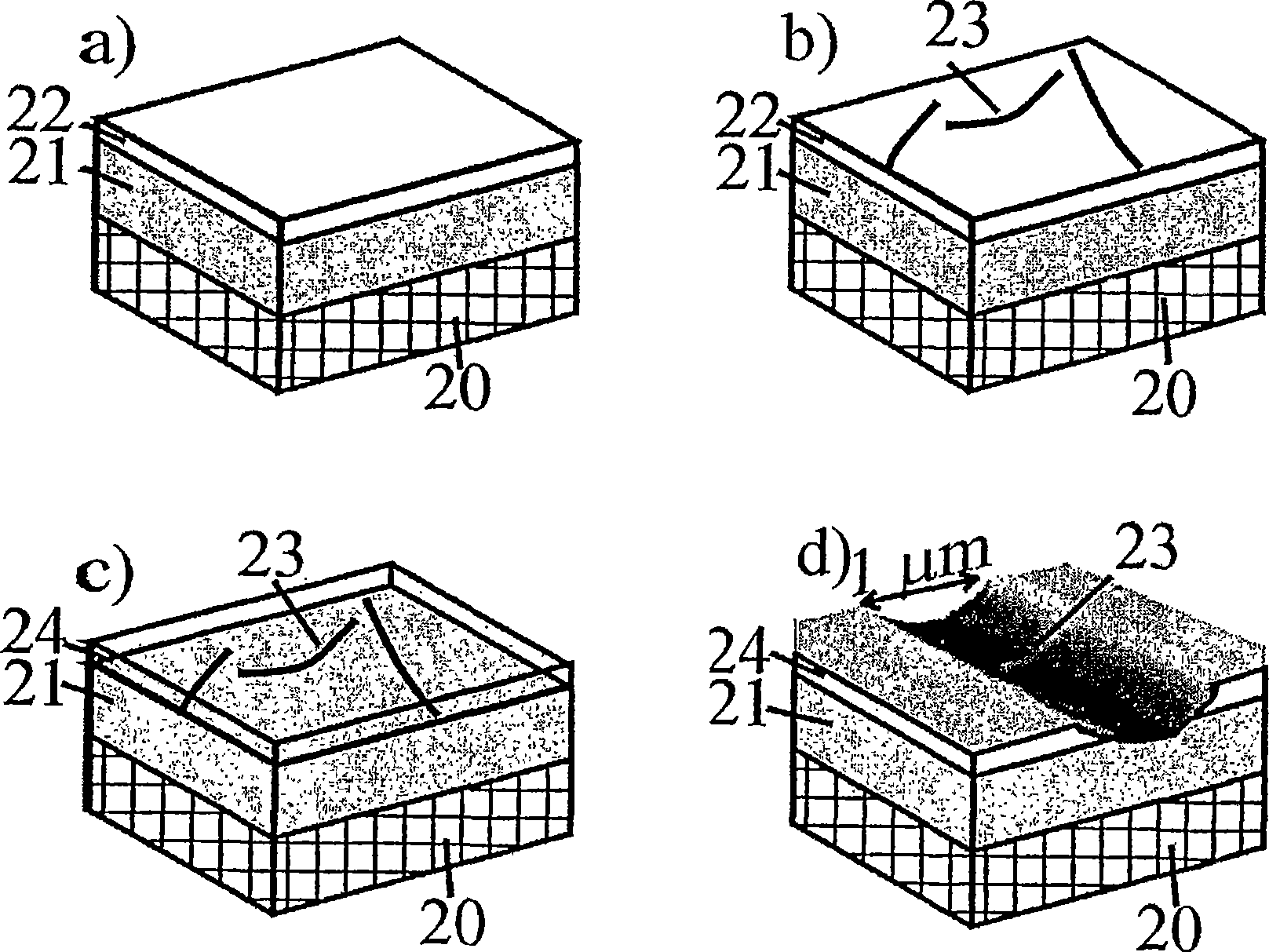
[0085] refer to figure 1 , 2 and 3, illustrate the main process steps involved in the fabrication of a simple device and an example of a simple device, namely the fabrication of a field effect transistor (FET).

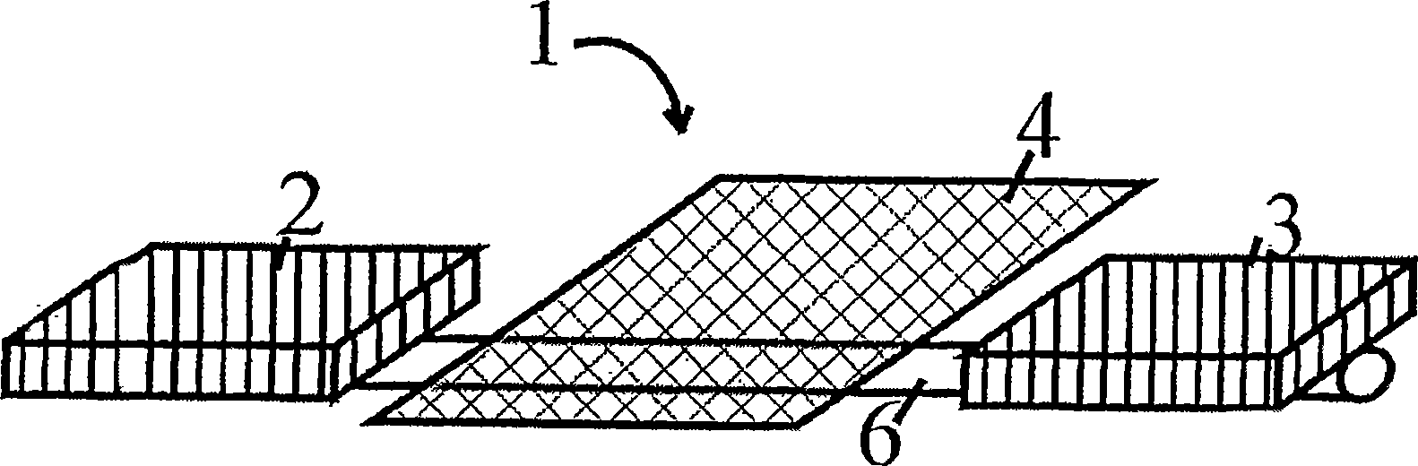
[0086] figure 1 Denotes FET part 1. The device is a three terminal device comprising a source 2 and drain 3 and a gate 4 electrically connected to wires (not shown). Electromagnetic semiconductor material for source and drain - Ga 1-x mn x As (GaMnAs), but may also be made of other materials suitable for semiconductors. The source 2 and the drain 3 are connected through a single-walled nanotube 6 . The electrodes of source 2, drain 3 and gate 4 may be semiconductor elements formed from the epitaxial layer above the nanotubes. A single electronic transistor device can be obtained with a similar design.

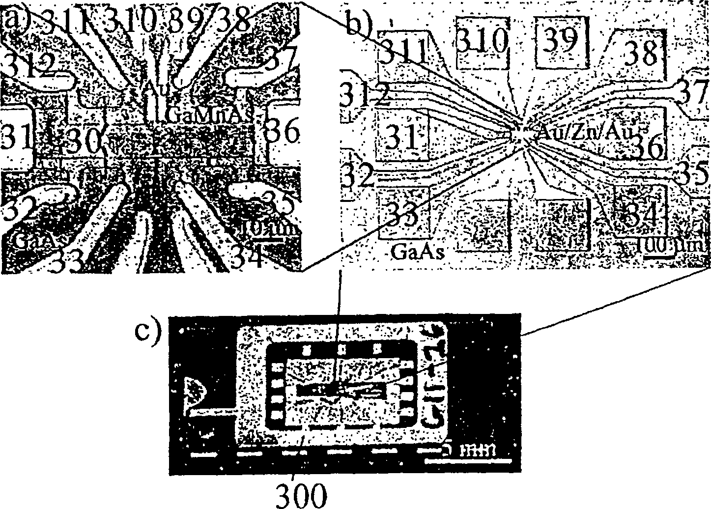
[0087] now refer to fig...


PUM

PropertyMeasurementUnit
thicknessaaaaaaaaaa
thicknessaaaaaaaaaa
thicknessaaaaaaaaaa

Abstract

A method of fabricating a device comprising elongated nanoscale elements and such a device is disclosed. The device comprises an epitaxially grown layer into which elongated nanoscale elements such as carbon nanotubes are embedded. A substrate is provided supporting the epitaxial growth of the epitaxial layer, on which the elongated nanoscale element is placed and grown epitaxially through the epitaxial layer. The elongated nanoscale element is thus at least partially encapsulated by the epitaxially grown layer. One or more features are produced in this layer, the one or more features being produced by lithographic methods. Devices using carbon nanotubes as active elements can thus be provided. The method is applicable to hybrid devices that are mixed between conventional semiconductor devices and nanodevices.

Description

technical field [0001] The present invention relates to devices comprising elongated nanoscale elements and to the manufacture of such devices. The device comprises an epitaxially grown layer with elongated nanoscale elements such as carbon nanotubes. Background technique [0002] Since the advent of integrated circuits and computer chips, the performance of these devices has been increasing at a remarkable rate, advances driven primarily by advances in the miniaturization of the basic elements of integrated circuits and the ability to increase the density of elements in a chip such that integrated electronic devices per unit area able to perform more functions. However, this technology is already approaching the limits of what is possible with the miniaturization of conventional components such as Metal Oxide Field Effect Transistors (MOSFETs). For example, geometries are approaching their limits for heat dissipation and structural stability due to material diffusion, whi...

Claims


Application Information

Patent Timeline
Patent Type & Authority Applications(China)
IPC IPC(8): H01L21/00C30B25/02C30B25/18C30B33/00
CPCB82Y20/00C30B25/02C30B25/18
Inventor 乔纳斯·拉尔夫·豪普特曼阿尼·珍森波尔·埃里克·格雷格斯·汉森·林德罗夫杰斯波·尼杰拉德贾纳兹·萨多斯基
Owner UNIVERSITY OF COPENHAGEN
Why Eureka
Try Eureka