
Design and methods for measuring analytes using nanofabricated device

a nanofabricated device and analyte technology, applied in the field of measuring analytes, can solve the problems of amplification process, high cost, short read length, etc., and achieve the effect of short read length, high accuracy, and high accuracy

Active Publication Date: 2018-05-03
ROCHE MOLECULAR SYST INC
View PDF6 Cites 12 Cited by
  • Summary
  • Abstract
  • Description
  • Claims
  • Application Information

AI Technical Summary

Benefits of technology

The invention provides improved devices, methods, and systems for sequencing linear biomolecules at the single-molecule level using quantum tunneling effects. The devices have a precisely formed gap between two electrodes, which can detect changes in quantum tunneling current when a nucleobase or amino acid is present in the gap. The width of the gap can be nanodimensioned and can correspond to the size of the linear molecule being sequenced. The methods can involve deposition techniques such as atomic layer deposition or chemical vapor deposition, and the devices can be used to sequentially measure the changes in quantum tunneling current or voltage when a nucleobase or amino acid is present in the gap. The invention provides faster and more accurate sequencing of linear biomolecules and can be used in various applications such as genomics and proteomics.

Problems solved by technology

Such amplification processes, however, are generally associated with high costs, replicative sequencing being required for high accuracy, short read lengths, and a long turnaround time per run (TTR).
Although such single-molecule sequencing methods overcome some of the drawbacks of earlier generation amplification methods, they nevertheless retain certain disadvantages such as low resolution which in turn requires replicative sequencing.
None of the other electrodes in the array, however, may have a gap with the precise spacing required.

Method used


Image

  • Design and methods for measuring analytes using nanofabricated device
  • Design and methods for measuring analytes using nanofabricated device
  • Design and methods for measuring analytes using nanofabricated device

Examples


Embodiment Construction

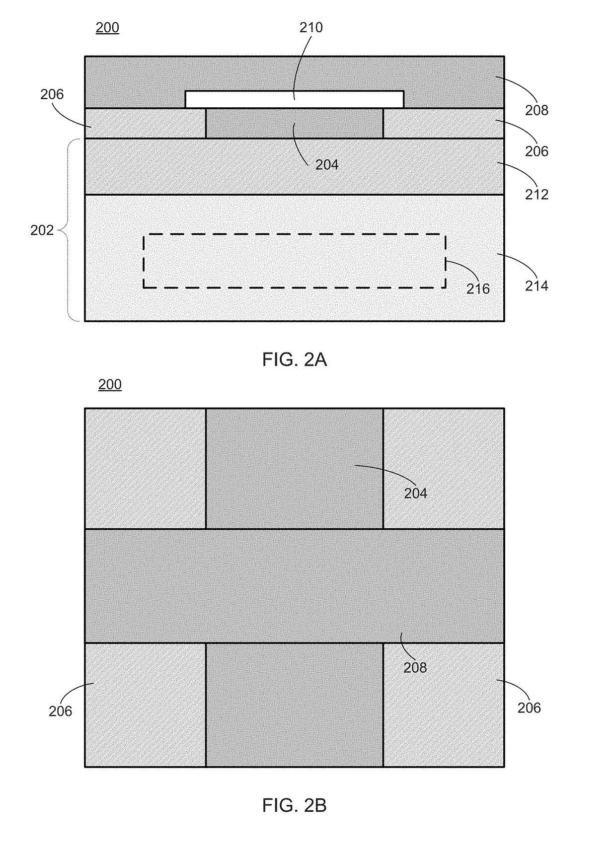
[0040]Embodiments can provide improved devices, methods of making devices, and methods of using devices, for sequencing linear biomolecules at the single-molecule level using quantum tunneling effects. In some embodiments, a nanofabricated device is provided including a precisely formed gap disposed between two electrodes and having a very small width (e.g., 0.8 to 5.0 nm). The width of the gap can correspond to the size of a linear biomolecule such as DNA, RNA, a polypeptide, a protein, and the like. When a part of the linear biomolecule (e.g., a nucleobase or amino acid) is present in the gap and a voltage is applied across the electrodes, a change in quantum tunneling current (or voltage) can be measured. The magnitude of the change can be mapped to the particular biomolecule part present at the time of measurement. As the linear biomolecule (or molecular fragment) traverses the gap, sequencing can be performed by taking subsequent measurements at time intervals selected based up...


PUM

PropertyMeasurementUnit
widthaaaaaaaaaa
sizeaaaaaaaaaa
width ofaaaaaaaaaa

Abstract

Devices for sequencing linear biomolecules (e.g., DNA, RNA, polypeptides, proteins, and the like) using quantum tunneling effects, and methods of making and using such devices, are provided. A nanofabricated device can include a small gap formed by depositing a thin film between two electrodes, and subsequently removing the film using an etching process. The width of the resulting gap can correspond with the size of a linear biomolecule such that when a part of the biomolecule (e.g., a nucleobase or amino acid) is present in the gap, a change in tunneling current, voltage, or impedance can be measured and the part of the biomolecule identified. The gap dimensions can be precisely controlled at the atomic-scale by, for example, atomic layer deposition (ALD) of the sacrificial film. The device can be made using existing integrated circuit fabrication equipment and facilities, and multiple devices can be formed on a single chip.

Description

CROSS-REFERENCE TO RELATED APPLICATIONS[0001]This patent application is a continuation of International Patent Application No. PCT / EP2016 / 065155 filed Jun. 29, 2016, which claims priority to and the benefit of U.S. Provisional Application No. 62 / 187,161, filed Jun. 30, 2015. Each of the above patent applications is incorporated herein by reference as if set forth in its entirety.FIELD[0002]This disclosure is generally related to measuring analytes, and more specifically to sequencing linear biomolecules (e.g., DNA, RNA, proteins, and the like) by a nanofabricated device using quantum tunneling effects.BACKGROUND[0003]In genetics, the term sequencing may refer to methods for determining a primary structure or sequence of a linear biomolecule such as DNA, RNA, amino acids, etc. For example, DNA sequencing is the process of determining an order of nucleobases (adenine, guanine, cytosine and thymine) in a given DNA fragment. DNA sequencing is a powerful method to reveal genetic variatio...

Claims


Application Information

Patent Timeline
Patent Type & Authority Applications(United States)
IPC IPC(8): G01N33/487G01N27/447C12Q1/6869
CPCG01N33/48721G01N27/44791C12Q1/6869C12Q2565/631
Inventor HENCK, STEVEN
Owner ROCHE MOLECULAR SYST INC
Learn More