Semiconductor memory

Active Publication Date: 2018-05-03
LAPIS SEMICON CO LTD
View PDF1 Cites 0 Cited by
  • Summary
  • Abstract
  • Description
  • Claims
  • Application Information

AI Technical Summary

Benefits of technology

The present invention provides a semiconductor memory that can prevent noise between bit lines and reduce the number of wiring layers, thus reducing manufacturing costs and the area of the device. The semiconductor memory has separate regions for complementary reading and reading using a reference signal, and noise is reduced through the use of shield lines in the complementary reading region. By providing the lower bit lines, upper bit lines, and shield lines in the same wiring layer and in separate positions, the propagation of noise between bit lines is suppressed while preventing an increase in device size.

Problems solved by technology

Thus, the number of wiring layers increases, resulting in an increase in manufacturing costs as well as the area.
Also, while the method of preventing noise by setting deselected bit lines at ground potential is effective in the case of a memory where reading is performed using a reference signal (1T1C type), this method cannot be used for a memory in which complementary reading is performed, where there are no deselected bit lines (2T2C type).
Therefore, this method could not be applied to a semiconductor memory that includes both a memory region where reading is performed using a reference signal and a memory region where complementary reading is performed.

Method used


Image

  • Semiconductor memory
  • Semiconductor memory
  • Semiconductor memory

Examples


embodiment 1

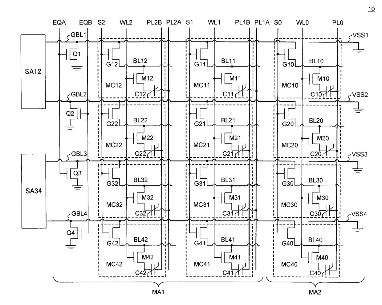
[0015]FIG. 1 is a circuit block diagram showing a semiconductor memory 10 according to the present invention. The semiconductor memory 10 has a first memory region MA1 and a second memory region MA2.

[0016]The first memory region MA1 has pairs of plate lines connected alternately to memory cells arranged in the column direction, and is a memory region where data is read by comparing a signal from a memory cell with a reference signal (hereinafter referred to as reading using a reference signal). The second memory region MA2 has one plate line connected to the memory cells arranged in the column direction, and is a memory region where data is read by comparing complementary signals from pairs of memory cells (hereinafter referred to as complementary reading). In other words, the first memory region MA1 is a so-called 1T1C-type memory region, and the second memory region MA2 is a so-called 2T2C-type memory region.

[0017]In the first memory region MA1, upper bit lines GBL1 to GBL4 are fo...

embodiment 2

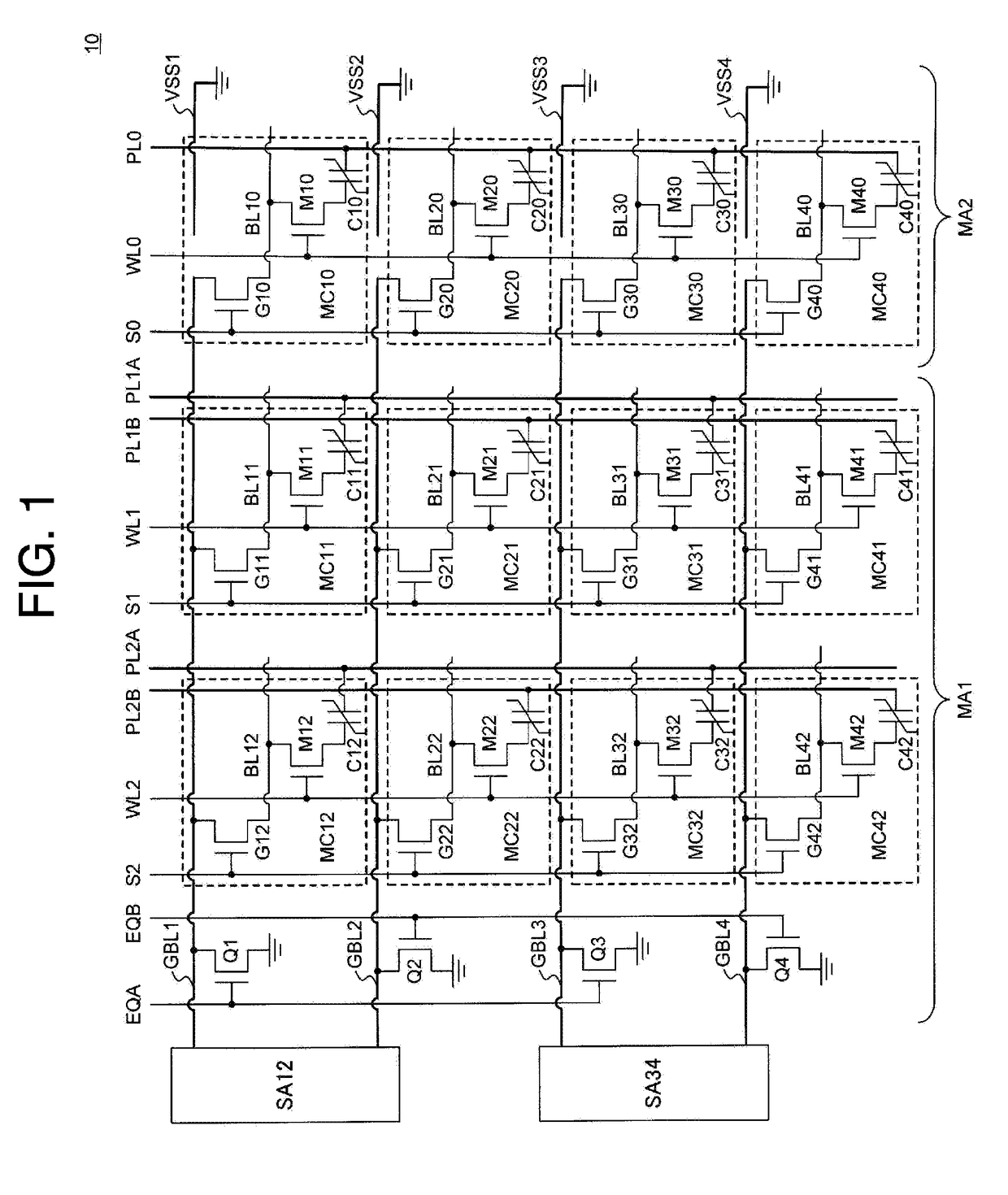
[0064]FIG. 2 is a circuit block diagram showing a semiconductor memory 20 according to the present invention. The semiconductor memory 20 differs from the semiconductor memory 10 of Embodiment 1 by having bit line discharge transistors Q11, Q12, Q21, Q22, Q31, Q32, Q41, and Q42.

[0065]In the bit line discharge transistor Q11, the drain terminal is connected to a lower bit line BL11, and the source terminal is grounded. In the bit line discharge transistor Q21, the drain terminal is connected to a lower bit line BL21, and the source terminal is grounded. In the bit line discharge transistor Q31, the drain terminal is connected to a lower bit line BL31, and the source terminal is grounded. In the bit line discharge transistor Q41, the drain terminal is connected to a lower bit line BL41, and the source terminal is grounded. In the bit line discharge transistor Q12, the drain terminal is connected to a lower bit line BL12, and the source terminal is grounded. In the bit line discharge t...

embodiment 3

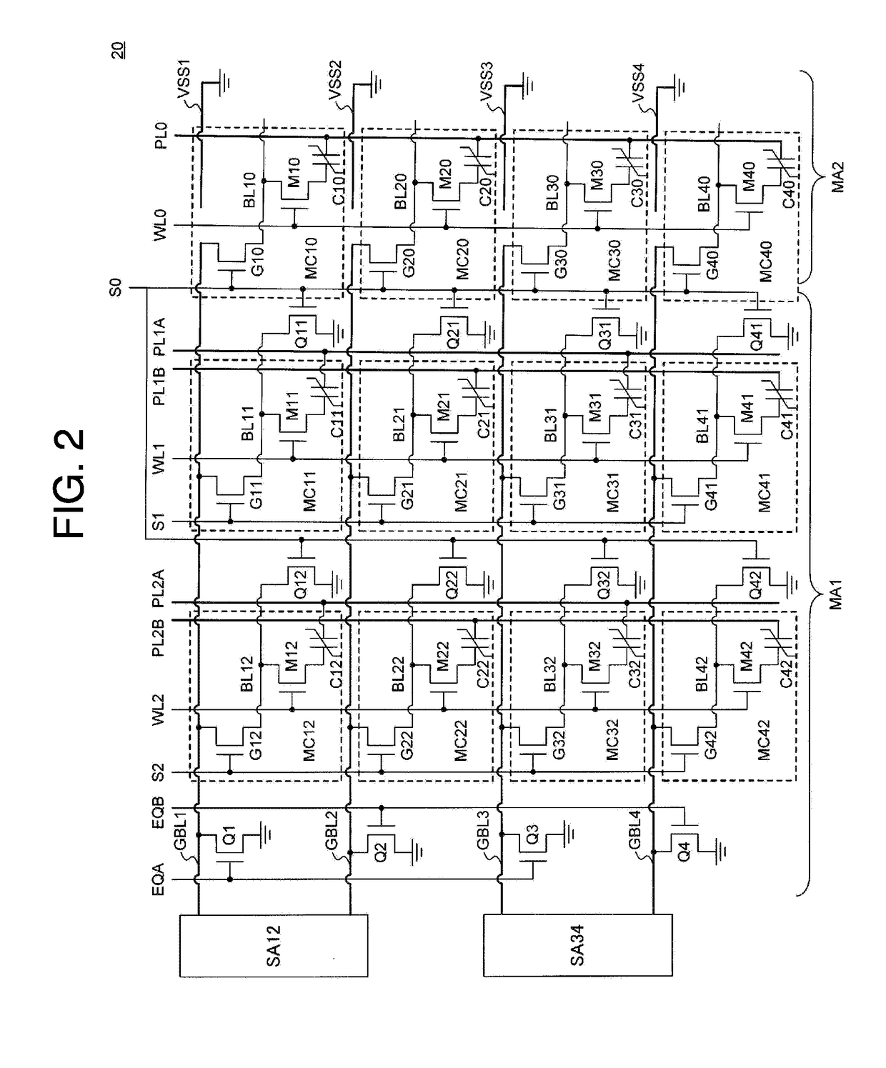
[0073]FIG. 3 is a circuit block diagram showing a semiconductor memory 30 according to the present invention. The semiconductor memory 30 differs from the semiconductor memory 10 of Embodiment 1, which only has one plate line PL0 in the second memory region MA2, in that the semiconductor memory 30 has a pair of plate lines PL0A and PL0B in the second memory region MA2.

[0074]The plate line PL0A is connected to the second terminals (ends not connected to memory cell transistors) of ferroelectric capacitors C10 and C30. The plate line PL0B is connected to the second terminals of ferroelectric capacitors C20 and C40. In other words, in the semiconductor memory 10 of Embodiment 1, the ferroelectric capacitors C10, C20, C30, and C40 are all connected to the same plate line PL0, whereas in the semiconductor memory 30 of the present embodiment, every other ferroelectric capacitors C10, C20, C30, and C40 is connected alternately to the plate lines PL0A and PL0B.

[0075]The plate lines PL0A and...


PUM


Abstract

A semiconductor memory includes j×k first memory cells, j upper bit lines, (½)j sense amplifiers, j×k lower first bit lines, k first word lines, k pairs of plate lines, each pair having first and second plate lines, each being connected to odd-numbered and even-numbered first memory cells of one of the k columns, a pair of discharge signal lines having a first discharge signal line and a second discharge signal line respectively connecting two of the j upper lines in each sense amplifier to a prescribed potential, j×m second memory cells, j lower second bit lines, m second word lines, m third plate lines each connected to the j second memory cells of one of the m columns, and j shield lines each provided at positions respectively corresponding to the j upper bit lines, which are parallel to one another.

Description

TECHNICAL FIELD[0001]The present invention relates to a semiconductor memory device.BACKGROUND ART[0002]As a non-volatile semiconductor storage device, a ferroelectric memory (ferroelectric random access memory: FeRAM) that uses a ferroelectric material as a capacitor is known. Ferroelectric memories are categorized into a 1T1C type in which data is read by comparing a reference signal and a signal from one memory cell constituted of a transistor and a ferroelectric capacitor, and a 2T2C type in which data is read by comparing complementary signals from a set of two memory cells (hereinafter referred to as complementary reading). In recent years, storage devices in which a 1T1C memory region and a 2T2C memory region coexist are known (Japanese Patent Application Laid-Open Publication No. 2016-54012, for example).[0003]In a semiconductor memory such as a ferroelectric memory, a plurality of bit lines are provided in parallel with each other. As a result, when reading from the memory,...

Claims


Application Information

Patent Timeline
IPC IPC(8): G11C11/4091G11C11/22G11C5/10G11C11/4094G11C11/4097G11C11/408G11C5/06G11C7/06
CPCG11C11/4091G11C11/221G11C5/10G11C11/4094G11C11/4097G11C11/4085G11C5/063G11C7/06G11C11/2255G11C5/025G11C7/02G11C7/12G11C7/18G11C11/2273G11C11/2259
Inventor YAMADA, TAKASHI
Owner LAPIS SEMICON CO LTD
Why Eureka
Try Eureka