Pulse width filtering circuit

a filtering circuit and pulse width technology, applied in the direction of logic circuits characterised by logic functions, pulse techniques, electronic switching, etc., can solve the problems of small pulse width signals in electronic circuits, and achieve the effects of improving circuit balance, logic gates, and reliable performan

Active Publication Date: 2018-05-03
MOSWAY TECH LTD
View PDF2 Cites 6 Cited by
  • Summary
  • Abstract
  • Description
  • Claims
  • Application Information

AI Technical Summary

Benefits of technology

[0012]Preferably, the first delay circuit and the second delay circuit have the same construction. The circuit symmetry improves circuit balance.
[0013]Preferably, the input transition detection circuit comprises one or more logic gates. Logic gates are relatively cheap and have reliable performance.
[0014]Preferably, the one or more logic gates comprises a NOR gate and a NAND gate, both arranged to receive the input signal and an output signal of the pulse width filtering circuit as input. By taking both the input signal and the output as input, the change of state can be more reliably determined.

Problems solved by technology

Electronic circuits are prone to small pulse width signals (“glitches”).

Method used


Image

  • Pulse width filtering circuit
  • Pulse width filtering circuit
  • Pulse width filtering circuit

Examples


Embodiment Construction

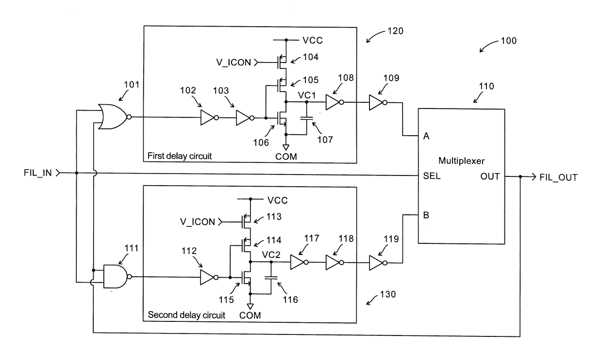
[0022]FIG. 1 shows a pulse width filtering circuit 100 in one embodiment of the invention. The pulse width filtering circuit 100 includes an input transition detection circuit arranged to detect change of state (transition from a low signal to a high signal, and vice versa) of an input signal at input FIL_IN, a delay circuit formed by two delay circuits each connected with the input transition detection circuit, and a switching circuit connected with the delay circuits to provide an output at FIL_OUT.

[0023]The input transition detection circuit includes a NOR gate 101 and a NAND gate 111, which are arranged to distinguish between rising edge (transition from low level to high level) and falling edge (transition from high level to low level) of the input signal. The NOR gate 101 takes the input signal at FIL_IN and the output signal at FIL_OUT as input. The NAND gate 111 likewise takes the input signal at FIL_IN and the output signal at FIL_OUT as input. The pin of the NAND gate 111 ...


PUM


Abstract

A pulse width filtering circuit for filtering pulse signals includes an input transition detection circuit detecting change of state of an input signal, including a first transition from a low signal to a high signal and a second transition from the high signal to the low signal; a first delay circuit determining whether the high signal from the first transition is maintained longer than a first period and, if so, generating a first output indicative of the first transition, after the first period; a second delay circuit determining whether the low signal from the second transition is maintained for longer than a second period and, if so, generating a second output indicative of the second transition, after the second period; and a switching circuit connected to the first and second delay circuits and selectively outputting the first output and the second output, based on the state of the input signal.

Description

TECHNICAL FIELD[0001]The invention relates to a pulse width filtering circuit, i.e., a filter circuit for processing or filtering pulse signals (input signals in the form of pulses).BACKGROUND[0002]Electronic circuits are prone to small pulse width signals (“glitches”). These small pulse width signals may be present at the interface of various integrated circuit components in a circuit. The propagation of these signals may have negative impact on circuit operation and performance, and so it is desirable that these signals be filtered, regulated, or controlled.SUMMARY OF THE INVENTION[0003]In accordance with a first aspect of the invention, there is provided a pulse width filtering circuit, comprising: an input transition detection circuit arranged to detect change of state of an input signal, the change of state comprising a first transition from a low signal to a high signal and a second transition from the high signal to the low signal; and a delay circuit operably connected with ...

Claims


Application Information

Patent Timeline
Patent Type & Authority Applications(United States)
IPC IPC(8): H03K5/156H03K5/1534H03K5/134
CPCH03K5/1565H03K5/1534H03K5/134H03K17/005H03K19/20
Inventor CHAN, ON BON PETER
Owner MOSWAY TECH LTD
Why Eureka
Try Eureka